Hu Hongpo, Zhou Shengjun, Wan Hui, Liu Xingtong, Li Ning, Xu Haohao
Center for Photonics and Semiconductors, School of Power and Mechanical Engineering, Wuhan University, Wuhan, 430072, China.
State Key Laboratory of Applied Optics, Changchun Institute of Optics, Fine Mechanics and Physics, Chinese Academy of Sciences, Changchun, 130033, China.
Sci Rep. 2019 Mar 5;9(1):3447. doi: 10.1038/s41598-019-40120-9.
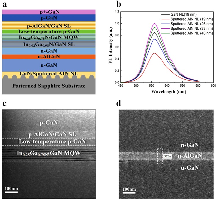
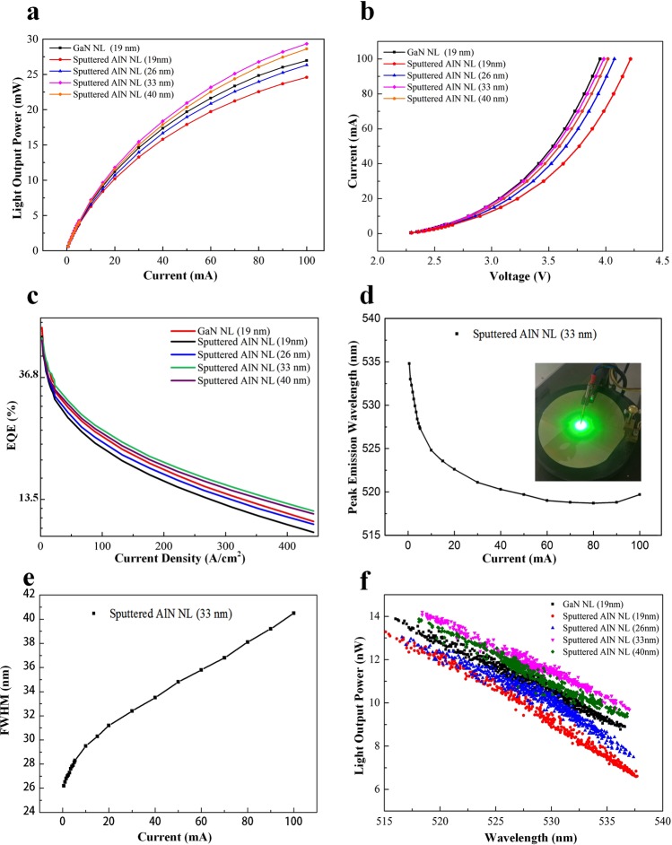
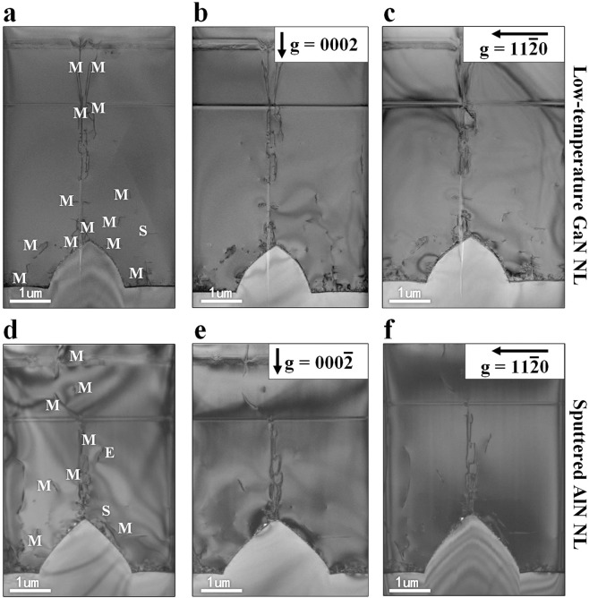
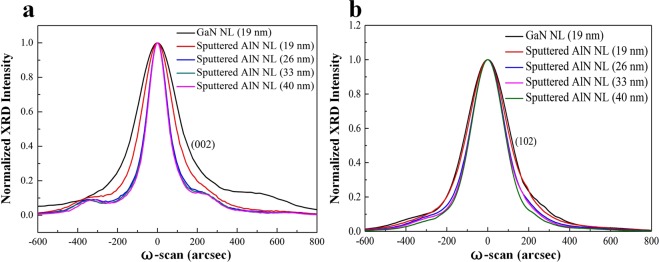
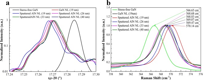
Here we demonstrate high-brightness InGaN/GaN green light emitting diodes (LEDs) with in-situ low-temperature GaN (LT-GaN) nucleation layer (NL) and ex-situ sputtered AlN NL on 4-inch patterned sapphire substrate. Compared to green LEDs on LT-GaN (19 nm)/sapphire template, green LEDs on sputtered AlN (19 nm)/template has better crystal quality while larger in-plane compressive strain. As a result, the external quantum efficiency (EQE) of green LEDs on sputtered AlN (19 nm)/sapphire template is lower than that of green LEDs on LT-GaN (19 nm)/sapphire template due to strain-induced quantum-confined Stark effect (QCSE). We show that the in-plane compressive strain of green LEDs on sputtered AlN/sapphire templates can be manipulated by changing thickness of the sputtered AlN NL. As the thickness of sputtered AlN NL changes from 19 nm to 40 nm, the green LED on sputtered AlN (33 nm)/sapphire template exhibits the lowest in-plane compressive stress and the highest EQE. At 20 A/cm, the EQE of 526 nm green LEDs on sputtered AlN (33 nm)/sapphire template is 36.4%, about 6.1% larger than that of the green LED on LT-GaN (19 nm)/sapphire template. Our experimental data suggest that high-efficiency green LEDs can be realized by growing InGaN/GaN multiple quantum wells (MQWs) on sputtered AlN/sapphire template with reduced in-plane compressive strain and improved crystal quality.
在此,我们展示了在4英寸图案化蓝宝石衬底上具有原位低温GaN(LT-GaN)成核层(NL)和异位溅射AlN NL的高亮度InGaN/GaN绿色发光二极管(LED)。与LT-GaN(19纳米)/蓝宝石模板上的绿色LED相比,溅射AlN(19纳米)/模板上的绿色LED具有更好的晶体质量,但面内压缩应变更大。因此,由于应变诱导的量子限制斯塔克效应(QCSE),溅射AlN(19纳米)/蓝宝石模板上的绿色LED的外量子效率(EQE)低于LT-GaN(19纳米)/蓝宝石模板上的绿色LED。我们表明,可以通过改变溅射AlN NL的厚度来控制溅射AlN/蓝宝石模板上绿色LED的面内压缩应变。随着溅射AlN NL的厚度从19纳米变为40纳米,溅射AlN(33纳米)/蓝宝石模板上的绿色LED表现出最低的面内压缩应力和最高的EQE。在20 A/cm时,溅射AlN(33纳米)/蓝宝石模板上526纳米绿色LED的EQE为36.4%,比LT-GaN(19纳米)/蓝宝石模板上的绿色LED大约6.1%。我们的实验数据表明,通过在具有降低的面内压缩应变和改善的晶体质量的溅射AlN/蓝宝石模板上生长InGaN/GaN多量子阱(MQW),可以实现高效绿色LED。