Min Lee Seung, Hwan Yum Jung, Larsen Eric S, Chul Lee Woo, Keun Kim Seong, Bielawski Christopher W, Oh Jungwoo
School of Integrated Technology, Yonsei University, Incheon, 21983, Republic of Korea.
Yonsei Institute of Convergence Technology, Incheon, 21983, Republic of Korea.
Sci Rep. 2017 Oct 16;7(1):13205. doi: 10.1038/s41598-017-13693-6.
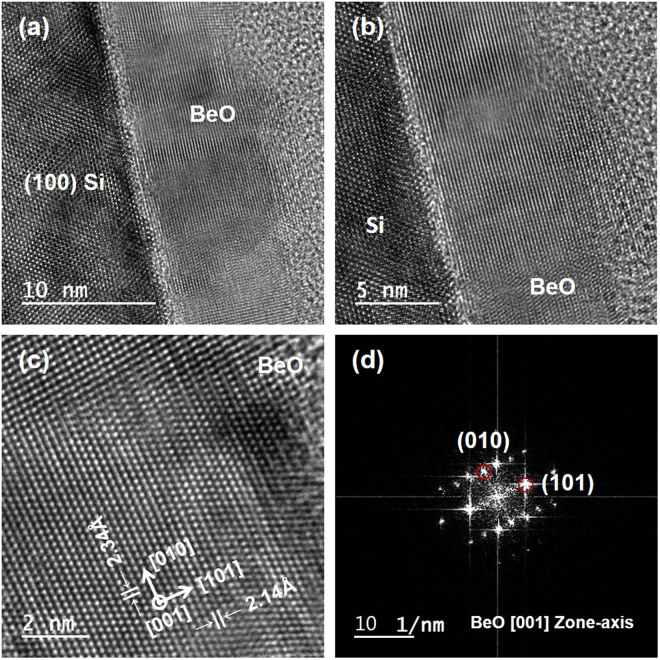
Silicon-on-insulator (SOI) technology improves the performance of devices by reducing parasitic capacitance. Devices based on SOI or silicon-on-sapphire technology are primarily used in high-performance radio frequency (RF) and radiation sensitive applications as well as for reducing the short channel effects in microelectronic devices. Despite their advantages, the high substrate cost and overheating problems associated with complexities in substrate fabrication as well as the low thermal conductivity of silicon oxide prevent broad applications of this technology. To overcome these challenges, we describe a new approach of using beryllium oxide (BeO). The use of atomic layer deposition (ALD) for producing this material results in lowering the SOI wafer production cost. Furthermore, the use of BeO exhibiting a high thermal conductivity might minimize the self-heating issues. We show that crystalline Si can be grown on ALD BeO and the resultant devices exhibit potential for use in advanced SOI technology applications.
绝缘体上硅(SOI)技术通过降低寄生电容来提高器件性能。基于SOI或蓝宝石上硅技术的器件主要用于高性能射频(RF)和辐射敏感应用,以及减少微电子器件中的短沟道效应。尽管它们具有优势,但与衬底制造复杂性相关的高衬底成本和过热问题,以及氧化硅的低导热性阻碍了该技术的广泛应用。为了克服这些挑战,我们描述了一种使用氧化铍(BeO)的新方法。使用原子层沉积(ALD)来生产这种材料可降低SOI晶圆的生产成本。此外,使用具有高导热性的BeO可能会使自热问题最小化。我们表明,可以在ALD BeO上生长晶体硅,并且所得器件具有用于先进SOI技术应用的潜力。