Centre for OptoElectronics and Biophotonics, School of Electrical and Electronic Engineering & The Photonics Institute, Nanyang Technological University, 50 Nanyang Avenue, Singapore, 639798, Singapore.
Centre for Programmable Materials, School of Materials Science and Engineering, Nanyang Technological University, 50 Nanyang Avenue, Singapore, 637371, Singapore.
Nat Commun. 2018 Apr 18;9(1):1545. doi: 10.1038/s41467-018-03935-0.
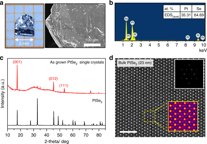
The interest in mid-infrared technologies surrounds plenty of important optoelectronic applications ranging from optical communications, biomedical imaging to night vision cameras, and so on. Although narrow bandgap semiconductors, such as Mercury Cadmium Telluride and Indium Antimonide, and quantum superlattices based on inter-subband transitions in wide bandgap semiconductors, have been employed for mid-infrared applications, it remains a daunting challenge to search for other materials that possess suitable bandgaps in this wavelength range. Here, we demonstrate experimentally for the first time that two-dimensional (2D) atomically thin PtSe has a variable bandgap in the mid-infrared via layer and defect engineering. Here, we show that bilayer PtSe combined with defects modulation possesses strong light absorption in the mid-infrared region, and we realize a mid-infrared photoconductive detector operating in a broadband mid-infrared range. Our results pave the way for atomically thin 2D noble metal dichalcogenides to be employed in high-performance mid-infrared optoelectronic devices.
人们对中红外技术的兴趣围绕着许多重要的光电应用,包括光通信、生物医学成像、夜视摄像机等。虽然窄带隙半导体,如汞镉碲化物和砷化铟锑,以及基于宽带隙半导体中的子带间跃迁的量子超晶格,已经被用于中红外应用,但寻找具有合适带隙的其他材料仍然是一个艰巨的挑战。在这里,我们首次通过层和缺陷工程实验证明,二维(2D)原子薄的 PtSe 具有中红外波段的可变带隙。在这里,我们表明,双层 PtSe 与缺陷调制相结合,在中红外区域具有很强的光吸收,并且我们实现了在宽带中红外范围内工作的中红外光电导探测器。我们的研究结果为原子薄的二维贵金属二硫化物在高性能中红外光电设备中的应用铺平了道路。