Lo Faro Maria José, Leonardi Antonio Alessio, Morganti Dario, Fazio Barbara, Vasi Ciro, Musumeci Paolo, Priolo Francesco, Irrera Alessia
MATIS IMM-CNR, Institute for Microelectronics and Microsystems, Via Santa Sofia 64, 95123 Catania, Italy.
IPCF-CNR, Institute for Chemical and Physical Processes, Viale F. Stagno D'Alcontres 37, 98158 Messina, Italy.
Nanomaterials (Basel). 2018 Jul 25;8(8):569. doi: 10.3390/nano8080569.
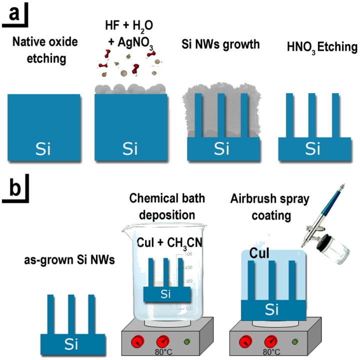
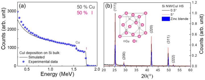
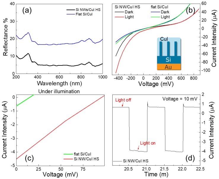
In this paper, we present the realization by a low cost approach compatible with silicon technology of new nanostructures, characterized by the presence of different materials, such as copper iodide (CuI) and silicon nanowires (Si NWs). Silicon is the principal material of the microelectronics field for its low cost, easy manufacturing and market stability. In particular, Si NWs emerged in the literature as the key materials for modern nanodevices. Copper iodide is a direct wide bandgap -type semiconductor used for several applications as a transparent hole conducting layers for dye-sensitized solar cells, light emitting diodes and for environmental purification. We demonstrated the preparation of a solid system in which Si NWs are embedded in CuI material and the structural, electrical and optical characterization is presented. These new combined Si NWs/CuI systems have strong potentiality to obtain new nanostructures characterized by different doping, that is strategic for the possibility to realize junction device. Moreover, the combination of these different materials opens the route to obtain multifunction devices characterized by promising absorption, light emission, and electrical conduction.
在本文中,我们展示了一种通过与硅技术兼容的低成本方法来实现新型纳米结构,这些纳米结构的特征在于存在不同的材料,如碘化铜(CuI)和硅纳米线(Si NWs)。硅因其低成本、易于制造和市场稳定性,是微电子领域的主要材料。特别是,硅纳米线在文献中已成为现代纳米器件的关键材料。碘化铜是一种直接宽带隙型半导体,用作染料敏化太阳能电池的透明空穴传导层、发光二极管以及用于环境净化等多种应用。我们展示了一种固态系统的制备,其中硅纳米线嵌入碘化铜材料中,并给出了结构、电学和光学表征。这些新的硅纳米线/碘化铜组合系统具有很强的潜力来获得具有不同掺杂特性的新型纳米结构,这对于实现结型器件的可能性具有重要意义。此外,这些不同材料的组合为获得具有良好吸收、发光和导电特性的多功能器件开辟了道路。