Leonardi Antonio Alessio, Faro Maria José Lo, Irrera Alessia
Dipartimento di Fisica e Astronomia "Ettore Majorana", Università di Catania, Via Santa Sofia 64, 95123 Catania, Italy.
Consiglio Nazionale delle Ricerche-Instituto Processi Chimico-Fisici (CNR-IPCF), Viale F. Stagno D'Alcontres 37, 98158 Messina, Italy.
Nanomaterials (Basel). 2021 Feb 3;11(2):383. doi: 10.3390/nano11020383.
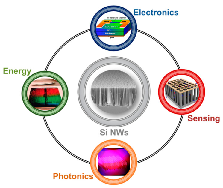
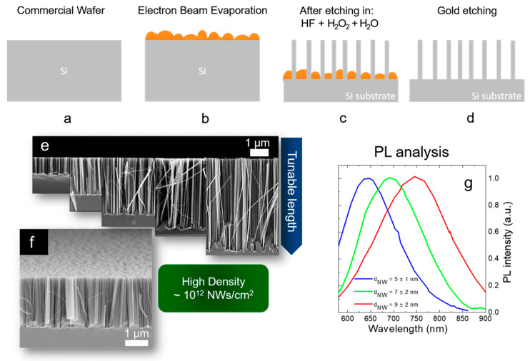
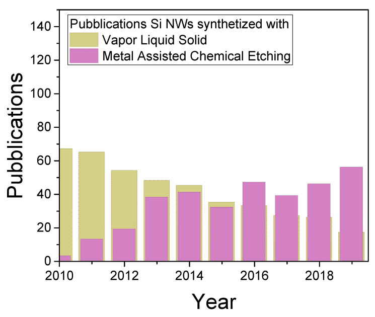
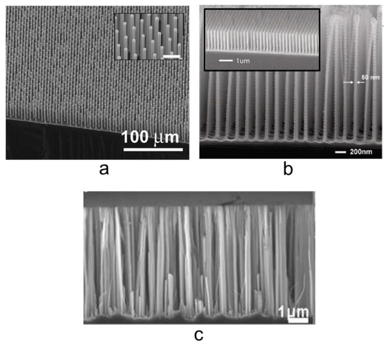
Silicon is the undisputed leader for microelectronics among all the industrial materials and Si nanostructures flourish as natural candidates for tomorrow's technologies due to the rising of novel physical properties at the nanoscale. In particular, silicon nanowires (Si NWs) are emerging as a promising resource in different fields such as electronics, photovoltaic, photonics, and sensing. Despite the plethora of techniques available for the synthesis of Si NWs, metal-assisted chemical etching (MACE) is today a cutting-edge technology for cost-effective Si nanomaterial fabrication already adopted in several research labs. During these years, MACE demonstrates interesting results for Si NW fabrication outstanding other methods. A critical study of all the main MACE routes for Si NWs is here presented, providing the comparison among all the advantages and drawbacks for different MACE approaches. All these fabrication techniques are investigated in terms of equipment, cost, complexity of the process, repeatability, also analyzing the possibility of a commercial transfer of these technologies for microelectronics, and which one may be preferred as industrial approach.
在所有工业材料中,硅无疑是微电子领域的佼佼者。由于纳米尺度下新物理特性的出现,硅纳米结构作为未来技术的天然候选材料蓬勃发展。特别是,硅纳米线(Si NWs)正在成为电子、光伏、光子学和传感等不同领域中一种有前途的资源。尽管有大量可用于合成硅纳米线的技术,但金属辅助化学蚀刻(MACE)如今是一种前沿技术,用于经济高效地制造硅纳米材料,已在多个研究实验室中采用。这些年来,MACE在硅纳米线制造方面展现出优于其他方法的有趣成果。本文对硅纳米线的所有主要MACE路线进行了批判性研究,比较了不同MACE方法的所有优缺点。所有这些制造技术都从设备、成本、工艺复杂性、可重复性等方面进行了研究,还分析了这些技术向微电子领域商业转移的可能性,以及哪种技术可能更适合作为工业方法。