• 文献检索
  • 文档翻译
  • 深度研究
  • 学术资讯
  • Suppr Zotero 插件Zotero 插件
  • 邀请有礼
  • 套餐&价格
  • 历史记录
应用&插件
Suppr Zotero 插件Zotero 插件浏览器插件Mac 客户端Windows 客户端微信小程序
定价
高级版会员购买积分包购买API积分包
服务
文献检索文档翻译深度研究API 文档MCP 服务
关于我们
关于 Suppr公司介绍联系我们用户协议隐私条款
关注我们

Suppr 超能文献

核心技术专利:CN118964589B侵权必究
粤ICP备2023148730 号-1Suppr @ 2026

文献检索

告别复杂PubMed语法,用中文像聊天一样搜索,搜遍4000万医学文献。AI智能推荐,让科研检索更轻松。

立即免费搜索

文件翻译

保留排版,准确专业,支持PDF/Word/PPT等文件格式,支持 12+语言互译。

免费翻译文档

深度研究

AI帮你快速写综述,25分钟生成高质量综述,智能提取关键信息,辅助科研写作。

立即免费体验

用于量子技术的单晶金刚石膜的先进制造

Advanced Fabrication of Single-Crystal Diamond Membranes for Quantum Technologies.

作者信息

Challier Michel, Sonusen Selda, Barfuss Arne, Rohner Dominik, Riedel Daniel, Koelbl Johannes, Ganzhorn Marc, Appel Patrick, Maletinsky Patrick, Neu Elke

机构信息

Fachrichtung Physik, Universität des Saarlandes, 66123 Saarbrücken, Germany.

Department of Physics, University of Basel, Klingelbergstrasse 82, CH-4056 Basel, Switzerland.

出版信息

Micromachines (Basel). 2018 Mar 25;9(4):148. doi: 10.3390/mi9040148.

DOI:10.3390/mi9040148
PMID:30424082
原文链接:https://pmc.ncbi.nlm.nih.gov/articles/PMC6187842/
Abstract

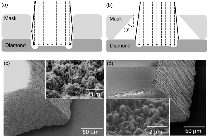
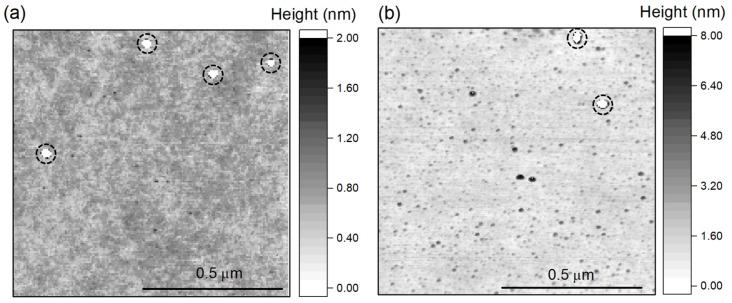
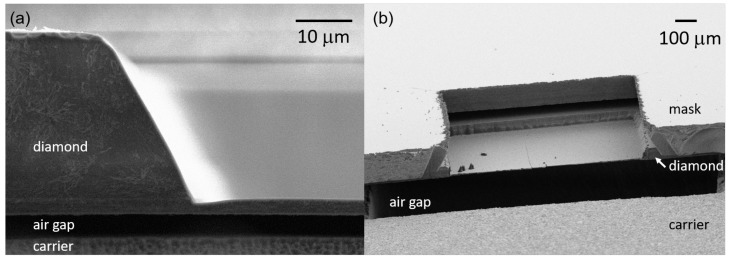
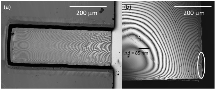
Many promising applications of single crystal diamond and its color centers as sensor platform and in photonics require free-standing membranes with a thickness ranging from several micrometers to the few 100 nm range. In this work, we present an approach to conveniently fabricate such thin membranes with up to about one millimeter in size. We use commercially available diamond plates (thickness 50 μ m) in an inductively coupled reactive ion etching process which is based on argon, oxygen and SF 6 . We thus avoid using toxic, corrosive feed gases and add an alternative to previously presented recipes involving chlorine-based etching steps. Our membranes are smooth (RMS roughness <1 nm) and show moderate thickness variation (central part: <1 μ m over ≈200 × 200 μ m 2 ). Due to an improved etch mask geometry, our membranes stay reliably attached to the diamond plate in our chlorine-based as well as SF 6 -based processes. Our results thus open the route towards higher reliability in diamond device fabrication and up-scaling.

摘要

单晶金刚石及其色心作为传感器平台以及在光子学领域的许多有前景的应用都需要厚度在几微米到几百纳米范围内的独立式薄膜。在这项工作中,我们提出了一种方便地制造尺寸达约一毫米的此类薄膜的方法。我们在基于氩气、氧气和六氟化硫的电感耦合反应离子蚀刻工艺中使用市售的金刚石板(厚度50μm)。因此,我们避免使用有毒、腐蚀性的进料气体,并为先前提出的涉及氯基蚀刻步骤的方法提供了一种替代方案。我们的薄膜很光滑(均方根粗糙度<1nm),并且显示出适度的厚度变化(中心部分:在约200×200μm²范围内<1μm)。由于蚀刻掩模几何形状的改进,我们的薄膜在基于氯的工艺以及基于六氟化硫的工艺中都能可靠地附着在金刚石板上。因此,我们的结果为提高金刚石器件制造的可靠性和扩大规模开辟了道路。

https://cdn.ncbi.nlm.nih.gov/pmc/blobs/7c42/6187842/93c781ffe3a1/micromachines-09-00148-g004.jpg
https://cdn.ncbi.nlm.nih.gov/pmc/blobs/7c42/6187842/8ee113d6217f/micromachines-09-00148-g001.jpg
https://cdn.ncbi.nlm.nih.gov/pmc/blobs/7c42/6187842/33b223f9a6dd/micromachines-09-00148-g002.jpg
https://cdn.ncbi.nlm.nih.gov/pmc/blobs/7c42/6187842/e2bb57c004dc/micromachines-09-00148-g003.jpg
https://cdn.ncbi.nlm.nih.gov/pmc/blobs/7c42/6187842/93c781ffe3a1/micromachines-09-00148-g004.jpg

相似文献

1
Advanced Fabrication of Single-Crystal Diamond Membranes for Quantum Technologies.用于量子技术的单晶金刚石膜的先进制造
Micromachines (Basel). 2018 Mar 25;9(4):148. doi: 10.3390/mi9040148.
2
Fabrication and Characterization of Single-Crystal Diamond Membranes for Quantum Photonics with Tunable Microcavities.用于具有可调微腔的量子光子学的单晶金刚石膜的制备与表征
Micromachines (Basel). 2020 Dec 4;11(12):1080. doi: 10.3390/mi11121080.
3
Scalable fabrication of high-quality, ultra-thin single crystal diamond membrane windows.高质量超薄单晶金刚石膜窗口的可扩展制造。
Nanoscale. 2016 Mar 28;8(12):6860-5. doi: 10.1039/c5nr08348f.
4
Optically Coherent Nitrogen-Vacancy Centers in Micrometer-Thin Etched Diamond Membranes.微米级薄蚀刻金刚石膜中的光学相干氮空位中心
Nano Lett. 2019 Jun 12;19(6):3987-3992. doi: 10.1021/acs.nanolett.9b01316. Epub 2019 Jun 4.
5
Precision micro-mechanical components in single crystal diamond by deep reactive ion etching.通过深反应离子刻蚀制备的单晶金刚石精密微机械部件。
Microsyst Nanoeng. 2018 Jun 18;4:12. doi: 10.1038/s41378-018-0014-5. eCollection 2018.
6
Inverse-designed diamond photonics.逆设计金刚石光子学。
Nat Commun. 2019 Jul 25;10(1):3309. doi: 10.1038/s41467-019-11343-1.
7
Reliable Nanofabrication of Single-Crystal Diamond Photonic Nanostructures for Nanoscale Sensing.用于纳米级传感的单晶金刚石光子纳米结构的可靠纳米制造。
Micromachines (Basel). 2019 Oct 24;10(11):718. doi: 10.3390/mi10110718.
8
Scalable Fabrication of Integrated Nanophotonic Circuits on Arrays of Thin Single Crystal Diamond Membrane Windows.可扩展制造集成纳米光子电路在薄单晶金刚石膜窗口阵列上。
Nano Lett. 2016 May 11;16(5):3341-7. doi: 10.1021/acs.nanolett.6b00974. Epub 2016 Apr 27.
9
High- Nanophotonic Resonators on Diamond Membranes using Templated Atomic Layer Deposition of TiO.利用TiO的模板化原子层沉积在金刚石膜上制备的高纳米光子谐振器
Nano Lett. 2020 Jun 10;20(6):4603-4609. doi: 10.1021/acs.nanolett.0c01467. Epub 2020 May 28.
10
Single crystal diamond membranes for nanoelectronics.单晶金刚石膜用于纳电子学。
Nanoscale. 2018 Feb 22;10(8):4028-4035. doi: 10.1039/c7nr09097h.

引用本文的文献

1
A Review of Diamond Materials and Applications in Power Semiconductor Devices.金刚石材料及其在功率半导体器件中的应用综述。
Materials (Basel). 2024 Jul 11;17(14):3437. doi: 10.3390/ma17143437.
2
Fabrication and Characterization of Single-Crystal Diamond Membranes for Quantum Photonics with Tunable Microcavities.用于具有可调微腔的量子光子学的单晶金刚石膜的制备与表征
Micromachines (Basel). 2020 Dec 4;11(12):1080. doi: 10.3390/mi11121080.
3
Reliable Nanofabrication of Single-Crystal Diamond Photonic Nanostructures for Nanoscale Sensing.

本文引用的文献

1
Quantum Nonlinear Optics with a Germanium-Vacancy Color Center in a Nanoscale Diamond Waveguide.纳米级金刚石波导中锗空位色心的量子非线性光学
Phys Rev Lett. 2017 Jun 2;118(22):223603. doi: 10.1103/PhysRevLett.118.223603. Epub 2017 May 31.
2
Fabrication of all diamond scanning probes for nanoscale magnetometry.用于纳米级磁力测量的全金刚石扫描探针的制造。
Rev Sci Instrum. 2016 Jun;87(6):063703. doi: 10.1063/1.4952953.
3
Quantitative nanoscale vortex imaging using a cryogenic quantum magnetometer.使用低温量子磁力计进行定量纳米级涡旋成像。
用于纳米级传感的单晶金刚石光子纳米结构的可靠纳米制造。
Micromachines (Basel). 2019 Oct 24;10(11):718. doi: 10.3390/mi10110718.
4
Optically Coherent Nitrogen-Vacancy Centers in Micrometer-Thin Etched Diamond Membranes.微米级薄蚀刻金刚石膜中的光学相干氮空位中心
Nano Lett. 2019 Jun 12;19(6):3987-3992. doi: 10.1021/acs.nanolett.9b01316. Epub 2019 Jun 4.
Nat Nanotechnol. 2016 Aug;11(8):677-81. doi: 10.1038/nnano.2016.63. Epub 2016 May 2.
4
Scalable fabrication of high-quality, ultra-thin single crystal diamond membrane windows.高质量超薄单晶金刚石膜窗口的可扩展制造。
Nanoscale. 2016 Mar 28;8(12):6860-5. doi: 10.1039/c5nr08348f.
5
Strain coupling of a nitrogen-vacancy center spin to a diamond mechanical oscillator.氮空位中心自旋与金刚石机械振荡器的应变耦合。
Phys Rev Lett. 2014 Jul 11;113(2):020503. doi: 10.1103/PhysRevLett.113.020503. Epub 2014 Jul 10.
6
Magnetometry with nitrogen-vacancy defects in diamond.金刚石中的氮空位缺陷的磁力测量。
Rep Prog Phys. 2014 May;77(5):056503. doi: 10.1088/0034-4885/77/5/056503. Epub 2014 May 6.
7
Single-crystal diamond nanomechanical resonators with quality factors exceeding one million.单晶金刚石纳米机械谐振器的品质因数超过一百万。
Nat Commun. 2014 Apr 8;5:3638. doi: 10.1038/ncomms4638.
8
High-precision nanoscale temperature sensing using single defects in diamond.利用金刚石中的单缺陷进行高精度纳米尺度温度传感。
Nano Lett. 2013 Jun 12;13(6):2738-42. doi: 10.1021/nl401216y.
9
A robust scanning diamond sensor for nanoscale imaging with single nitrogen-vacancy centres.一种用于单氮空位中心纳米成像的稳健扫描金刚石传感器。
Nat Nanotechnol. 2012 Apr 15;7(5):320-4. doi: 10.1038/nnano.2012.50.
10
One- and two-dimensional photonic crystal microcavities in single crystal diamond.单晶金刚石中的一维和二维光子晶体微腔。
Nat Nanotechnol. 2011 Nov 13;7(1):69-74. doi: 10.1038/nnano.2011.190.