• 文献检索
  • 文档翻译
  • 深度研究
  • 学术资讯
  • Suppr Zotero 插件Zotero 插件
  • 邀请有礼
  • 套餐&价格
  • 历史记录
应用&插件
Suppr Zotero 插件Zotero 插件浏览器插件Mac 客户端Windows 客户端微信小程序
定价
高级版会员购买积分包购买API积分包
服务
文献检索文档翻译深度研究API 文档MCP 服务
关于我们
关于 Suppr公司介绍联系我们用户协议隐私条款
关注我们

Suppr 超能文献

核心技术专利:CN118964589B侵权必究
粤ICP备2023148730 号-1Suppr @ 2026

文献检索

告别复杂PubMed语法,用中文像聊天一样搜索,搜遍4000万医学文献。AI智能推荐,让科研检索更轻松。

立即免费搜索

文件翻译

保留排版,准确专业,支持PDF/Word/PPT等文件格式,支持 12+语言互译。

免费翻译文档

深度研究

AI帮你快速写综述,25分钟生成高质量综述,智能提取关键信息,辅助科研写作。

立即免费体验

双面聚合物表面纳米结构的电学性质

Electrical Properties of Double-Sided Polymer Surface Nanostructures.

作者信息

Zhang Man, Xia Liangping, Dang Suihu, Cao Axiu, Shi Lifang, Pang Hui, Du Chunlei

机构信息

School of Electronic Information Engineering, Yangtze Normal University, Chongqing, 408100, China.

Institute of Optics and Electronics, Chinese Academy of Sciences, Chengdu, 610209, China.

出版信息

Nanoscale Res Lett. 2019 Jul 11;14(1):230. doi: 10.1186/s11671-019-3071-2.

DOI:10.1186/s11671-019-3071-2
PMID:31297675
原文链接:https://pmc.ncbi.nlm.nih.gov/articles/PMC6624224/
Abstract

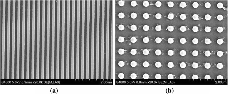
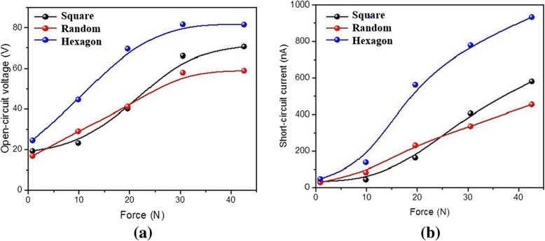
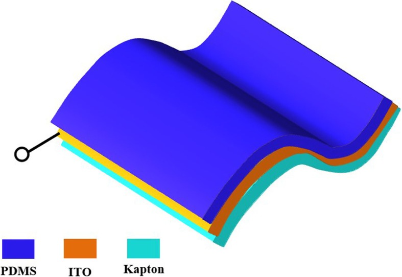
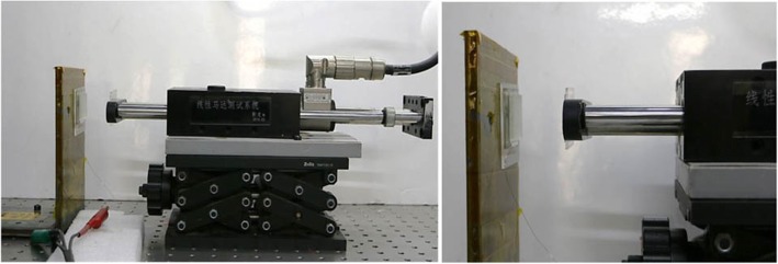
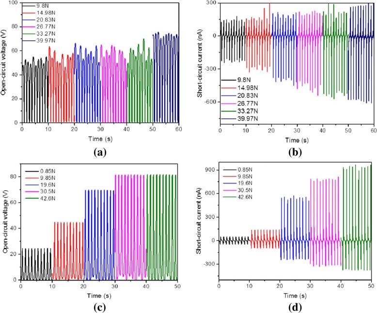
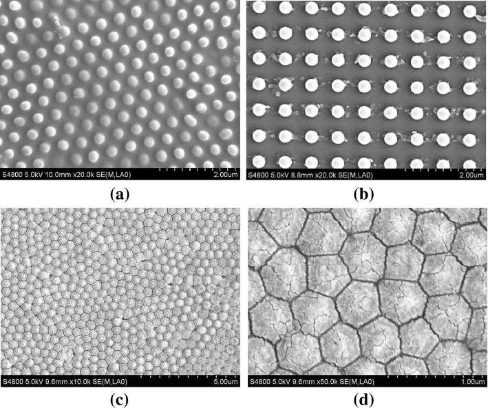
In this study, double-sided polymer surface nanostructures are fabricated using twice nanoimprint lithography and metal deposition technique. We perform electrical property measurement on these double-sided surface nanostructures. Open-circuit voltage and short-circuit current of the as-prepared samples with double-sided surface nanostructures and conductive electrode are recorded using an oscilloscope with applying different external force. The measurements are carried out at room temperature. We find that the intensity of open-circuit voltage and short-circuit current for the double-sided surface nanostructures depends strongly on the sizes, shapes, and arrangements of nanostructures and pressure force. The strongest electrical property can be observed in the hexagon nanopillar arrays with the diameter of about 400 nm containing sub-50-nm resolution sharp structures at the force of about 40 N. We discuss the physical mechanisms responsible for these interesting research findings. The experimental results we study are relevant to the applications of double-sided surface nanostructures such as a nanogenerator, pressure sensors, and nano-optoelectronic devices.

摘要

在本研究中,采用两次纳米压印光刻和金属沉积技术制备了双面聚合物表面纳米结构。我们对这些双面表面纳米结构进行了电学性能测量。使用示波器在施加不同外力的情况下,记录了具有双面表面纳米结构和导电电极的制备样品的开路电压和短路电流。测量在室温下进行。我们发现,双面表面纳米结构的开路电压和短路电流强度强烈依赖于纳米结构的尺寸、形状、排列以及压力。在直径约400nm、包含分辨率低于50nm的尖锐结构的六边形纳米柱阵列中,在约40N的力作用下可观察到最强的电学性能。我们讨论了导致这些有趣研究结果的物理机制。我们所研究的实验结果与双面表面纳米结构在纳米发电机、压力传感器和纳米光电器件等方面的应用相关。

https://cdn.ncbi.nlm.nih.gov/pmc/blobs/eeef/6624224/bcd753f486e5/11671_2019_3071_Fig6_HTML.jpg
https://cdn.ncbi.nlm.nih.gov/pmc/blobs/eeef/6624224/e2e4554e63a9/11671_2019_3071_Fig1_HTML.jpg
https://cdn.ncbi.nlm.nih.gov/pmc/blobs/eeef/6624224/2b50606811c3/11671_2019_3071_Fig2_HTML.jpg
https://cdn.ncbi.nlm.nih.gov/pmc/blobs/eeef/6624224/b7cb1ac18514/11671_2019_3071_Fig3_HTML.jpg
https://cdn.ncbi.nlm.nih.gov/pmc/blobs/eeef/6624224/f29a91cfbfd2/11671_2019_3071_Fig4_HTML.jpg
https://cdn.ncbi.nlm.nih.gov/pmc/blobs/eeef/6624224/c4bb518475ca/11671_2019_3071_Fig5_HTML.jpg
https://cdn.ncbi.nlm.nih.gov/pmc/blobs/eeef/6624224/bcd753f486e5/11671_2019_3071_Fig6_HTML.jpg

相似文献

1
Electrical Properties of Double-Sided Polymer Surface Nanostructures.双面聚合物表面纳米结构的电学性质
Nanoscale Res Lett. 2019 Jul 11;14(1):230. doi: 10.1186/s11671-019-3071-2.
2
Tribological Properties and Electrification Performance of Patterned Surface for Sliding-Mode Triboelectric Nanogenerator.用于滑模摩擦电纳米发电机的图案化表面的摩擦学性能和起电性能
Langmuir. 2019 Jul 23;35(29):9396-9401. doi: 10.1021/acs.langmuir.9b01020. Epub 2019 Jul 8.
3
Optical properties of Ni and Cu nanowire arrays and Ni/Cu superlattice nanowire arrays.镍和铜纳米线阵列及镍/铜超晶格纳米线阵列的光学性质。
Nanoscale Res Lett. 2012 Oct 15;7(1):569. doi: 10.1186/1556-276X-7-569.
4
Modulating Optical Characteristics of Nanoimprinted Plasmonic Device by Re-Shaping Process of Polymer Mold.通过聚合物模具的重塑工艺调控纳米压印等离子体器件的光学特性。
Micromachines (Basel). 2021 Oct 28;12(11):1323. doi: 10.3390/mi12111323.
5
Large area high density sub-20 nm SiO(2) nanostructures fabricated by block copolymer template for nanoimprint lithography.通过嵌段共聚物模板制备用于纳米压印光刻的大面积高密度亚20纳米二氧化硅纳米结构。
ACS Nano. 2009 Sep 22;3(9):2601-8. doi: 10.1021/nn900701p.
6
Fast switching behavior of nanoscale Ag6In5Sb59Te30 based nanopillar type phase change memory.基于纳米级 Ag6In5Sb59Te30 的纳米柱型相变存储器的快速切换行为。
Nanotechnology. 2010 Jan 15;21(2):025703. doi: 10.1088/0957-4484/21/2/025703. Epub 2009 Dec 3.
7
Electrical readouts of single and few molecule systems in metal-molecule-metal device structures.金属-分子-金属器件结构中单个及少数分子系统的电学读数。
J Nanosci Nanotechnol. 2007 Jun;7(6):2134-8. doi: 10.1166/jnn.2007.783.
8
Nanoimprint lithography-based replication techniques for fabrication of metal and polymer biomimetic nanostructures for biosensor surface functionalization.基于纳米压印光刻的复制技术,用于制造用于生物传感器表面功能化的金属和聚合物仿生纳米结构。
Nanotechnology. 2023 Feb 6;34(16). doi: 10.1088/1361-6528/acb35b.
9
Au nanostructure arrays for plasmonic applications: annealed island films versus nanoimprint lithography.用于等离子体应用的金纳米结构阵列:退火岛状薄膜与纳米压印光刻技术
Nanoscale Res Lett. 2015 Mar 1;10:99. doi: 10.1186/s11671-015-0819-1. eCollection 2015.
10
Nanoskiving: a new method to produce arrays of nanostructures.纳米切片:一种制备纳米结构阵列的新方法。
Acc Chem Res. 2008 Dec;41(12):1566-77. doi: 10.1021/ar700194y.

本文引用的文献

1
And There Was Light: Prospects for the Creation of Micro- and Nanostructures through Maskless Photolithography.《有光则明:掩模自由光刻技术制造微纳结构的前景》
ACS Nano. 2017 Sep 26;11(9):8537-8541. doi: 10.1021/acsnano.7b05593. Epub 2017 Sep 14.
2
Employing shells to eliminate concentration quenching in photonic upconversion nanostructure.采用壳层结构消除上转换纳米结构中的浓度猝灭。
Nanoscale. 2017 Jun 14;9(23):7941-7946. doi: 10.1039/c7nr01403a.
3
Continuous fabrication of nanostructure arrays for flexible surface enhanced Raman scattering substrate.
连续制造用于柔性表面增强拉曼散射衬底的纳米结构阵列。
Sci Rep. 2017 Jan 4;7:39814. doi: 10.1038/srep39814.
4
Fano resonances in the nonlinear optical response of coupled plasmonic nanostructures.耦合等离子体纳米结构非线性光学响应中的法诺共振
Opt Express. 2014 Dec 1;22(24):29693-707. doi: 10.1364/OE.22.029693.
5
Active micro-actuators for optical modulation based on a planar sliding triboelectric nanogenerator.基于平面滑动摩擦纳米发电机的光调制用主动微致动器。
Adv Mater. 2015 Jan 27;27(4):719-26. doi: 10.1002/adma.201404291. Epub 2014 Nov 27.
6
Magnetic tuning of plasmonic excitation of gold nanorods.金纳米棒等离子体激发的磁调谐。
J Am Chem Soc. 2013 Oct 16;135(41):15302-5. doi: 10.1021/ja408289b. Epub 2013 Oct 8.
7
Nanoscale triboelectric-effect-enabled energy conversion for sustainably powering portable electronics.基于纳米摩擦电效应的能量转换,可持续为便携式电子设备供电。
Nano Lett. 2012 Dec 12;12(12):6339-46. doi: 10.1021/nl303573d. Epub 2012 Nov 12.
8
A review on inorganic nanostructure self-assembly.无机纳米结构自组装综述。
J Nanosci Nanotechnol. 2010 Mar;10(3):1563-83. doi: 10.1166/jnn.2010.2030.
9
Surface plasmon resonance in a hexagonal nanostructure formed by seven core shell nanocylinders.由七个核壳纳米圆柱体形成的六边形纳米结构中的表面等离子体共振。
Appl Opt. 2010 Feb 10;49(5):920-6. doi: 10.1364/AO.49.000920.
10
Large-area roll-to-roll and roll-to-plate nanoimprint lithography: a step toward high-throughput application of continuous nanoimprinting.大面积卷对卷和卷对板纳米压印光刻技术:迈向连续纳米压印高通量应用的一步。
ACS Nano. 2009 Aug 25;3(8):2304-10. doi: 10.1021/nn9003633.