Lee Esther, Kim Tae Hyeon, Lee Seung Won, Kim Jee Hoon, Kim Jaeun, Jeong Tae Gun, Ahn Ji-Hoon, Cho Byungjin
Department of Advanced Material Engineering, Chungbuk National University, Chungbuk, 28644, Republic of Korea.
Department of Electronic Material Engineering, Korea Maritime and Ocean University, Busan, 49112, Republic of Korea.
Nano Converg. 2019 Jul 22;6(1):24. doi: 10.1186/s40580-019-0194-1.
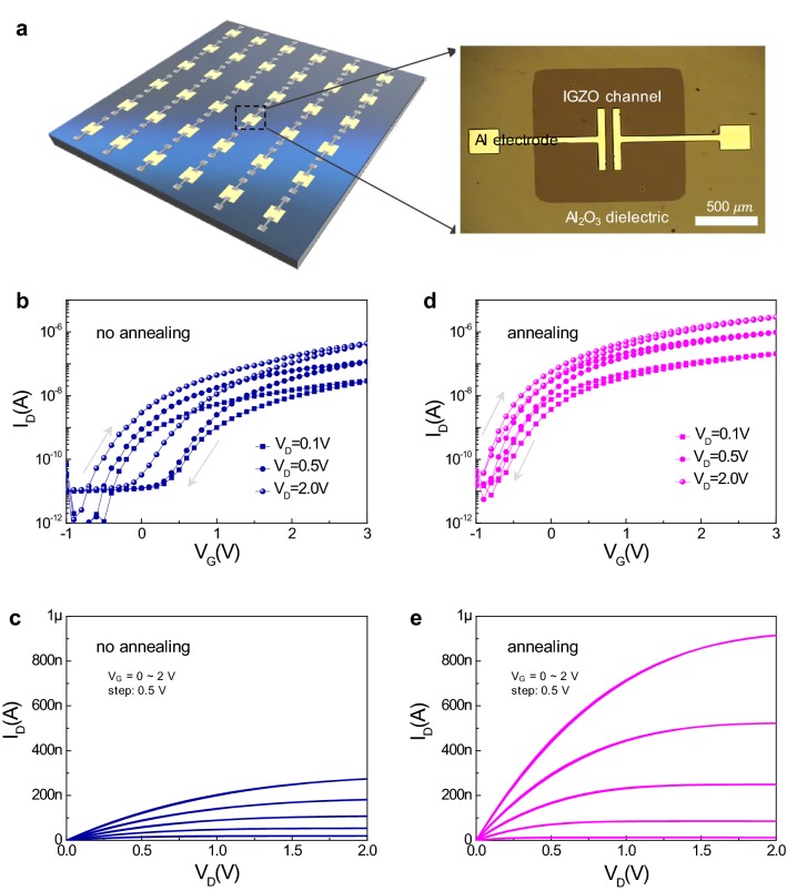
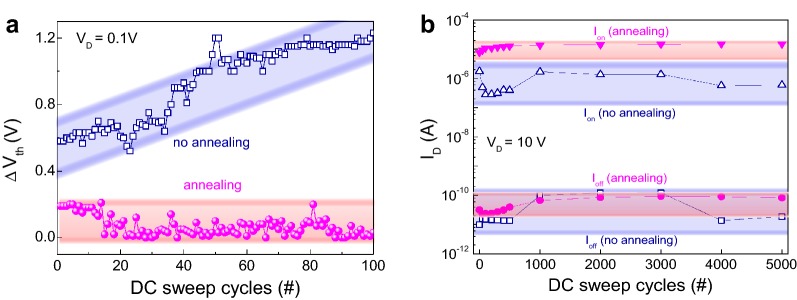
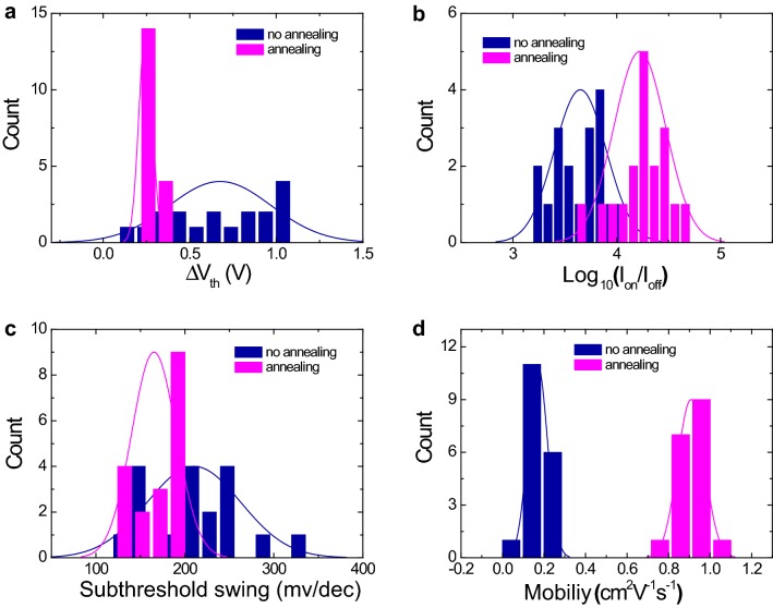
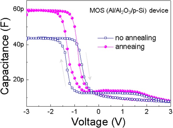
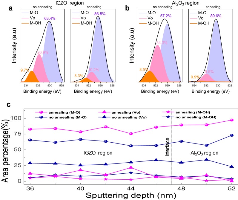
We have explored the effect of post-annealing on the electrical properties of an indium gallium zinc oxide (IGZO) transistor with an AlO bottom gate dielectric, formed by a sol-gel process. The post-annealed IGZO device demonstrated improved electrical performance in terms of threshold variation, on/off ratio, subthreshold swing, and mobility compared to the non-annealed reference device. Capacitance-voltage measurement confirmed that annealing can lead to enhanced capacitance properties due to reduced charge trapping. Depth profile analysis using X-ray photoelectron spectroscopy proved that percentage of both the oxygen vacancy (V) and the hydroxyl groups (M-OH) within the IGZO/AlO layers, which serve as a charge trapping source, can be substantially reduced by annealing the fabricated transistor device. Furthermore, the undesired degradation of the contact interface between source/drain electrode and the channel, which mainly concerns V, can be largely prevented by post-annealing. Thus, the facile annealing process also improves the electrical bias stress stability. This simple post annealing approach provides a strategy for realising better performance and reliability of the solid sol-gel oxide transistor.
我们研究了退火后处理对采用溶胶-凝胶工艺制备的、具有AlO底栅介质的铟镓锌氧化物(IGZO)晶体管电学性能的影响。与未退火的参考器件相比,退火后的IGZO器件在阈值变化、开/关比、亚阈值摆幅和迁移率方面展现出了更好的电学性能。电容-电压测量证实,退火可因电荷俘获减少而导致电容性能增强。利用X射线光电子能谱进行的深度剖析分析证明,通过对制备好的晶体管器件进行退火,可大幅降低作为电荷俘获源的IGZO/AlO层内氧空位(V)和羟基(M-OH)的百分比。此外,通过退火后处理可在很大程度上防止源/漏电极与沟道之间主要与V有关的接触界面出现不期望的退化。因此,这种简便的退火工艺还提高了电偏置应力稳定性。这种简单的退火后处理方法为实现固态溶胶-凝胶氧化物晶体管更好的性能和可靠性提供了一种策略。