• 文献检索
  • 文档翻译
  • 深度研究
  • 学术资讯
  • Suppr Zotero 插件Zotero 插件
  • 邀请有礼
  • 套餐&价格
  • 历史记录
应用&插件
Suppr Zotero 插件Zotero 插件浏览器插件Mac 客户端Windows 客户端微信小程序
定价
高级版会员购买积分包购买API积分包
服务
文献检索文档翻译深度研究API 文档MCP 服务
关于我们
关于 Suppr公司介绍联系我们用户协议隐私条款
关注我们

Suppr 超能文献

核心技术专利:CN118964589B侵权必究
粤ICP备2023148730 号-1Suppr @ 2026

文献检索

告别复杂PubMed语法,用中文像聊天一样搜索,搜遍4000万医学文献。AI智能推荐,让科研检索更轻松。

立即免费搜索

文件翻译

保留排版,准确专业,支持PDF/Word/PPT等文件格式,支持 12+语言互译。

免费翻译文档

深度研究

AI帮你快速写综述,25分钟生成高质量综述,智能提取关键信息,辅助科研写作。

立即免费体验

通过氩氧混合等离子体处理和快速热退火改善双栅铟镓锌氧化物薄膜晶体管的器件特性

Improving Device Characteristics of Dual-Gate IGZO Thin-Film Transistors with Ar-O Mixed Plasma Treatment and Rapid Thermal Annealing.

作者信息

Liu Wei-Sheng, Hsu Chih-Hao, Jiang Yu, Lai Yi-Chun, Kuo Hsing-Chun

机构信息

Department of Electrical Engineering, Yuan Ze University, Chung-Li 320, Taiwan.

Department of Nursing, Division of Basic Medical Sciences, Chang Gung University of Science and Technology, Chiayi 613, Taiwan.

出版信息

Membranes (Basel). 2021 Dec 30;12(1):49. doi: 10.3390/membranes12010049.

DOI:10.3390/membranes12010049
PMID:35054574
原文链接:https://pmc.ncbi.nlm.nih.gov/articles/PMC8780293/
Abstract

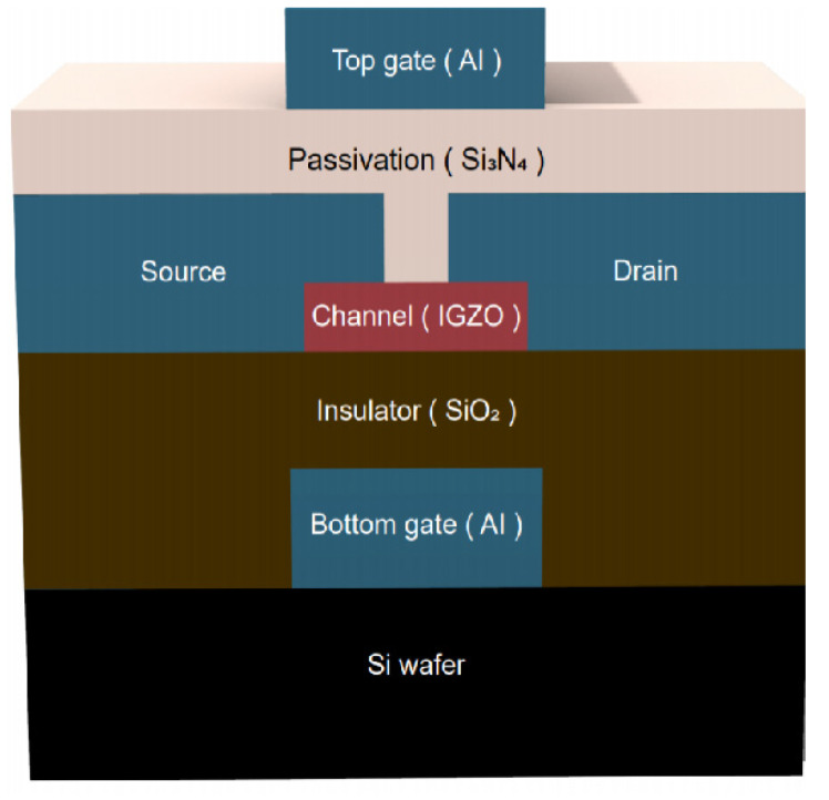
In this study, high-performance indium-gallium-zinc oxide thin-film transistors (IGZO TFTs) with a dual-gate (DG) structure were manufactured using plasma treatment and rapid thermal annealing (RTA). Atomic force microscopy measurements showed that the surface roughness decreased upon increasing the O ratio from 16% to 33% in the argon-oxygen plasma treatment mixture. Hall measurement results showed that both the thin-film resistivity and carrier Hall mobility of the Ar-O plasma-treated IGZO thin films increased with the reduction of the carrier concentration caused by the decrease in the oxygen vacancy density; this was also verified using X-ray photoelectron spectroscopy measurements. IGZO thin films treated with Ar-O plasma were used as channel layers for fabricating DG TFT devices. These DG IGZO TFT devices were subjected to RTA at 100 °C-300 °C for improving the device characteristics; the field-effect mobility, subthreshold swing, and I/I current ratio of the 33% O plasma-treated DG TFT devices improved to 58.8 cm/V·s, 0.12 V/decade, and 5.46 × 10, respectively. Long-term device stability reliability tests of the DG IGZO TFTs revealed that the threshold voltage was highly stable.

摘要

在本研究中,采用等离子体处理和快速热退火(RTA)制备了具有双栅(DG)结构的高性能铟镓锌氧化物薄膜晶体管(IGZO TFT)。原子力显微镜测量结果表明,在氩氧等离子体处理混合物中,随着氧比从16%增加到33%,表面粗糙度降低。霍尔测量结果表明,Ar-O等离子体处理的IGZO薄膜的薄膜电阻率和载流子霍尔迁移率均随着氧空位密度降低导致的载流子浓度降低而增加;这也通过X射线光电子能谱测量得到了验证。用Ar-O等离子体处理的IGZO薄膜用作制造DG TFT器件的沟道层。这些DG IGZO TFT器件在100℃至300℃下进行RTA以改善器件特性;33% O等离子体处理的DG TFT器件的场效应迁移率、亚阈值摆幅和I/I电流比分别提高到58.8 cm²/V·s、0.12 V/十倍频程和5.46×10⁷。DG IGZO TFT的长期器件稳定性可靠性测试表明,阈值电压非常稳定。

https://cdn.ncbi.nlm.nih.gov/pmc/blobs/b18a/8780293/0c5f68acd1ed/membranes-12-00049-g009.jpg
https://cdn.ncbi.nlm.nih.gov/pmc/blobs/b18a/8780293/e7e5f2d9396e/membranes-12-00049-g001.jpg
https://cdn.ncbi.nlm.nih.gov/pmc/blobs/b18a/8780293/81861e79b50e/membranes-12-00049-g002.jpg
https://cdn.ncbi.nlm.nih.gov/pmc/blobs/b18a/8780293/baaee72e9d93/membranes-12-00049-g003.jpg
https://cdn.ncbi.nlm.nih.gov/pmc/blobs/b18a/8780293/c5f023841321/membranes-12-00049-g004.jpg
https://cdn.ncbi.nlm.nih.gov/pmc/blobs/b18a/8780293/5e259880819e/membranes-12-00049-g005.jpg
https://cdn.ncbi.nlm.nih.gov/pmc/blobs/b18a/8780293/d4d4a5466e4e/membranes-12-00049-g006.jpg
https://cdn.ncbi.nlm.nih.gov/pmc/blobs/b18a/8780293/80a18279242d/membranes-12-00049-g007.jpg
https://cdn.ncbi.nlm.nih.gov/pmc/blobs/b18a/8780293/5b8258aacede/membranes-12-00049-g008.jpg
https://cdn.ncbi.nlm.nih.gov/pmc/blobs/b18a/8780293/0c5f68acd1ed/membranes-12-00049-g009.jpg

相似文献

1
Improving Device Characteristics of Dual-Gate IGZO Thin-Film Transistors with Ar-O Mixed Plasma Treatment and Rapid Thermal Annealing.通过氩氧混合等离子体处理和快速热退火改善双栅铟镓锌氧化物薄膜晶体管的器件特性
Membranes (Basel). 2021 Dec 30;12(1):49. doi: 10.3390/membranes12010049.
2
The effect of annealing ambient on the characteristics of an indium-gallium-zinc oxide thin film transistor.退火环境对铟镓锌氧化物薄膜晶体管特性的影响。
J Nanosci Nanotechnol. 2011 Jul;11(7):6029-33. doi: 10.1166/jnn.2011.4360.
3
Argon and Oxygen Gas Flow Rate Dependency of Sputtering-Based Indium-Gallium-Zinc Oxide Thin-Film Transistors.基于溅射的铟镓锌氧化物薄膜晶体管的氩气和氧气流量依赖性
Micromachines (Basel). 2023 Jul 8;14(7):1394. doi: 10.3390/mi14071394.
4
Performance Improvement of In-Ga-Zn Oxide Thin-Film Transistors by Excimer Laser Annealing.通过准分子激光退火提高铟镓锌氧化物薄膜晶体管的性能
Micromachines (Basel). 2024 Jan 31;15(2):225. doi: 10.3390/mi15020225.
5
Structural and electrical characteristics of high-κ Er2O3 and Er2TiO5 gate dielectrics for a-IGZO thin-film transistors.高介电常数 Er2O3 和 Er2TiO5 栅介质的结构和电学特性用于 a-IGZO 薄膜晶体管。
Nanoscale Res Lett. 2013 Jan 8;8(1):18. doi: 10.1186/1556-276X-8-18.
6
Intense Pulsed Light Annealing Process of Indium-Gallium-Zinc-Oxide Semiconductors via Flash White Light Combined with Deep-UV and Near-Infrared Drying for High-Performance Thin-Film Transistors.通过结合深紫外和近红外干燥的闪光白光对铟镓锌氧化物半导体进行高强度脉冲光退火工艺以制备高性能薄膜晶体管
ACS Appl Mater Interfaces. 2019 Apr 10;11(14):13380-13388. doi: 10.1021/acsami.8b22458. Epub 2019 Mar 27.
7
Enhanced Electrical Properties and Stability in IGZO TFTs via Low-Temperature Activation with MgO Layer.通过MgO层低温激活提高IGZO薄膜晶体管的电学性能和稳定性
ACS Appl Mater Interfaces. 2024 Aug 7;16(31):41127-41133. doi: 10.1021/acsami.4c06708. Epub 2024 Jul 26.
8
Study of the Correlation between the Amorphous Indium-Gallium-Zinc Oxide Film Quality and the Thin-Film Transistor Performance.非晶铟镓锌氧化物薄膜质量与薄膜晶体管性能之间的相关性研究。
Nanomaterials (Basel). 2021 Feb 18;11(2):522. doi: 10.3390/nano11020522.
9
Electrical Performance and Reliability Improvement of Amorphous-Indium-Gallium-Zinc-Oxide Thin-Film Transistors with HfO₂ Gate Dielectrics by CF₄ Plasma Treatment.通过CF₄等离子体处理改善具有HfO₂栅极电介质的非晶铟镓锌氧化物薄膜晶体管的电学性能和可靠性
Materials (Basel). 2018 May 17;11(5):824. doi: 10.3390/ma11050824.
10
Achieving a Low-Voltage, High-Mobility IGZO Transistor through an ALD-Derived Bilayer Channel and a Hafnia-Based Gate Dielectric Stack.通过原子层沉积法制备的双层沟道和基于氧化铪的栅极介质堆叠实现低电压、高迁移率铟镓锌氧化物晶体管。
ACS Appl Mater Interfaces. 2021 Apr 14;13(14):16628-16640. doi: 10.1021/acsami.0c22677. Epub 2021 Apr 1.

引用本文的文献

1
Selective Gelation Patterning of Solution-Processed Indium Zinc Oxide Films via Photochemical Treatments.通过光化学处理对溶液法制备的铟锌氧化物薄膜进行选择性凝胶图案化。
Nanomaterials (Basel). 2025 Jul 24;15(15):1147. doi: 10.3390/nano15151147.
2
Enhancing InGaZnO transistor current through high-κ dielectrics and interface trap extraction using single-pulse charge pumping.通过高κ电介质和使用单脉冲电荷泵的界面陷阱提取来增强铟镓锌氧化物晶体管电流。
Sci Rep. 2025 Jul 2;15(1):23113. doi: 10.1038/s41598-025-07995-3.
3
A tunable multi-timescale Indium-Gallium-Zinc-Oxide thin-film transistor neuron towards hybrid solutions for spiking neuromorphic applications.

本文引用的文献

1
Light response behaviors of amorphous In-Ga-Zn-O thin-film transistors interfacial hydrogen doping modulation.非晶铟镓锌氧化物薄膜晶体管界面氢掺杂调制的光响应行为
RSC Adv. 2020 Jan 22;10(6):3572-3578. doi: 10.1039/c9ra09646a. eCollection 2020 Jan 16.
2
Effects of Intense Pulsed Light (IPL) Rapid Annealing and Back-Channel Passivation on Solution-Processed In-Ga-Zn-O Thin Film Transistors Array.强脉冲光(IPL)快速退火和背沟道钝化对溶液法制备的铟镓锌氧化物薄膜晶体管阵列的影响
Micromachines (Basel). 2020 May 18;11(5):508. doi: 10.3390/mi11050508.
3
TFT Channel Materials for Display Applications: From Amorphous Silicon to Transition Metal Dichalcogenides.
一种用于尖峰神经形态应用的混合解决方案的可调谐多时间尺度铟镓锌氧化物薄膜晶体管神经元。
Commun Eng. 2024 Jul 23;3(1):102. doi: 10.1038/s44172-024-00248-7.
4
Effect of interface defects on electrical characteristics of a-ITGZO TFTs under bottom, top, and dual gatings.界面缺陷对底部、顶部和双栅极下非晶铟镓锌氧化物薄膜晶体管电学特性的影响。
Heliyon. 2024 Jul 4;10(13):e34134. doi: 10.1016/j.heliyon.2024.e34134. eCollection 2024 Jul 15.
5
Double-gate structure enabling remote Coulomb scattering-free transport in atomic-layer-deposited IGO thin-film transistors with HfO gate dielectric through insertion of SiO interlayer.通过插入SiO中间层,双栅结构可实现具有HfO栅极电介质的原子层沉积IGO薄膜晶体管中的远程无库仑散射传输。
Sci Rep. 2024 Apr 1;14(1):7623. doi: 10.1038/s41598-024-58330-1.
6
Effects of Source/Drain Electrodes on the Performance of InSnO Thin-Film Transistors.源极/漏极电极对InSnO薄膜晶体管性能的影响。
Micromachines (Basel). 2022 Nov 2;13(11):1896. doi: 10.3390/mi13111896.
7
Thin-Film Transistors.薄膜晶体管
Membranes (Basel). 2022 Apr 9;12(4):411. doi: 10.3390/membranes12040411.
用于显示应用的TFT沟道材料:从非晶硅到过渡金属二硫属化物。
Adv Mater. 2020 Sep;32(35):e1907166. doi: 10.1002/adma.201907166. Epub 2020 Mar 16.
4
Effects of Nitrogen and Hydrogen Codoping on the Electrical Performance and Reliability of InGaZnO Thin-Film Transistors.氮氢共掺杂对 InGaZnO 薄膜晶体管电性能和可靠性的影响。
ACS Appl Mater Interfaces. 2017 Mar 29;9(12):10798-10804. doi: 10.1021/acsami.6b15275. Epub 2017 Mar 15.
5
Transparent amorphous oxide semiconductors for organic electronics: Application to inverted OLEDs.用于有机电子学的透明非晶氧化物半导体:在倒置有机发光二极管中的应用。
Proc Natl Acad Sci U S A. 2017 Jan 10;114(2):233-238. doi: 10.1073/pnas.1617186114. Epub 2016 Dec 27.
6
Present status of amorphous In-Ga-Zn-O thin-film transistors.非晶铟镓锌氧化物薄膜晶体管的现状
Sci Technol Adv Mater. 2010 Sep 10;11(4):044305. doi: 10.1088/1468-6996/11/4/044305. eCollection 2010 Aug.
7
Oxygen vacancies promoting photoelectrochemical performance of In(2)O(3) nanocubes.氧空位促进 In(2)O(3)纳米立方体的光电化学性能。
Sci Rep. 2013;3:1021. doi: 10.1038/srep01021. Epub 2013 Jan 4.
8
Oxide semiconductor thin-film transistors: a review of recent advances.氧化物半导体薄膜晶体管:研究进展综述。
Adv Mater. 2012 Jun 12;24(22):2945-86. doi: 10.1002/adma.201103228. Epub 2012 May 10.
9
Materials and applications for large area electronics: solution-based approaches.大面积电子学的材料与应用:基于溶液的方法。
Chem Rev. 2010 Jan;110(1):3-24. doi: 10.1021/cr900150b.
10
Medium-scale carbon nanotube thin-film integrated circuits on flexible plastic substrates.柔性塑料基板上的中规模碳纳米管薄膜集成电路。
Nature. 2008 Jul 24;454(7203):495-500. doi: 10.1038/nature07110.