• 文献检索
  • 文档翻译
  • 深度研究
  • 学术资讯
  • Suppr Zotero 插件Zotero 插件
  • 邀请有礼
  • 套餐&价格
  • 历史记录
应用&插件
Suppr Zotero 插件Zotero 插件浏览器插件Mac 客户端Windows 客户端微信小程序
定价
高级版会员购买积分包购买API积分包
服务
文献检索文档翻译深度研究API 文档MCP 服务
关于我们
关于 Suppr公司介绍联系我们用户协议隐私条款
关注我们

Suppr 超能文献

核心技术专利:CN118964589B侵权必究
粤ICP备2023148730 号-1Suppr @ 2026

文献检索

告别复杂PubMed语法,用中文像聊天一样搜索,搜遍4000万医学文献。AI智能推荐,让科研检索更轻松。

立即免费搜索

文件翻译

保留排版,准确专业,支持PDF/Word/PPT等文件格式,支持 12+语言互译。

免费翻译文档

深度研究

AI帮你快速写综述,25分钟生成高质量综述,智能提取关键信息,辅助科研写作。

立即免费体验

由局部铁电极化实现的可重构二维光电器件。

Reconfigurable two-dimensional optoelectronic devices enabled by local ferroelectric polarization.

作者信息

Lv Liang, Zhuge Fuwei, Xie Fengjun, Xiong Xujing, Zhang Qingfu, Zhang Nan, Huang Yu, Zhai Tianyou

机构信息

State Key Laboratory of Materials Processing and Die & Mould Technology, School of Materials Science and Engineering, Huazhong University of Science and Technology, 430074, Wuhan, People's Republic of China.

出版信息

Nat Commun. 2019 Jul 26;10(1):3331. doi: 10.1038/s41467-019-11328-0.

DOI:10.1038/s41467-019-11328-0
PMID:31350401
原文链接:https://pmc.ncbi.nlm.nih.gov/articles/PMC6659647/
Abstract

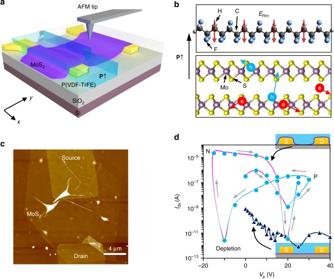
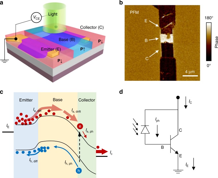
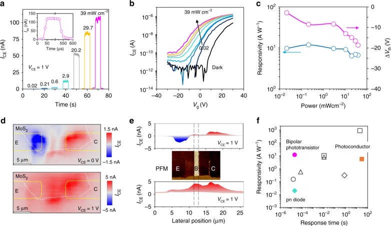
Ferroelectric engineered pn doping in two-dimensional (2D) semiconductors hold essential promise in realizing customized functional devices in a reconfigurable manner. Here, we report the successful pn doping in molybdenum disulfide (MoS) optoelectronic device by local patterned ferroelectric polarization, and its configuration into lateral diode and npn bipolar phototransistors for photodetection from such a versatile playground. The lateral pn diode formed in this way manifests efficient self-powered detection by separating ~12% photo-generated electrons and holes. When polarized as bipolar phototransistor, the device is customized with a gain ~1000 by its transistor action, reaching the responsivity ~12 A W and detectivity over 10 Jones while keeping a fast response speed within 20 μs. A promising pathway toward high performance optoelectronics is thus opened up based on local ferroelectric polarization coupled 2D semiconductors.

摘要

二维(2D)半导体中的铁电工程pn掺杂在以可重构方式实现定制功能器件方面具有重要前景。在此,我们报告了通过局部图案化铁电极化在二硫化钼(MoS)光电器件中成功实现pn掺杂,并将其配置为横向二极管和npn双极光电晶体管,用于从这个多功能平台进行光检测。以这种方式形成的横向pn二极管通过分离约12%的光生电子和空穴表现出高效的自供电检测。当极化作为双极光电晶体管时,该器件通过其晶体管作用定制增益约为1000,响应度达到约12 A/W,探测率超过10琼斯,同时在20 μs内保持快速响应速度。基于局部铁电极化耦合的二维半导体,由此开辟了一条通往高性能光电子学的有前途的途径。

https://cdn.ncbi.nlm.nih.gov/pmc/blobs/5d0a/6659647/27e577cee13c/41467_2019_11328_Fig6_HTML.jpg
https://cdn.ncbi.nlm.nih.gov/pmc/blobs/5d0a/6659647/faa641523d77/41467_2019_11328_Fig1_HTML.jpg
https://cdn.ncbi.nlm.nih.gov/pmc/blobs/5d0a/6659647/29217d786d55/41467_2019_11328_Fig2_HTML.jpg
https://cdn.ncbi.nlm.nih.gov/pmc/blobs/5d0a/6659647/dfa3874364ae/41467_2019_11328_Fig3_HTML.jpg
https://cdn.ncbi.nlm.nih.gov/pmc/blobs/5d0a/6659647/99bd87b2dc78/41467_2019_11328_Fig4_HTML.jpg
https://cdn.ncbi.nlm.nih.gov/pmc/blobs/5d0a/6659647/e3b5eb77a8ba/41467_2019_11328_Fig5_HTML.jpg
https://cdn.ncbi.nlm.nih.gov/pmc/blobs/5d0a/6659647/27e577cee13c/41467_2019_11328_Fig6_HTML.jpg

相似文献

1
Reconfigurable two-dimensional optoelectronic devices enabled by local ferroelectric polarization.由局部铁电极化实现的可重构二维光电器件。
Nat Commun. 2019 Jul 26;10(1):3331. doi: 10.1038/s41467-019-11328-0.
2
Broadband, Polarization-Sensitive, and Self-Powered High-Performance Photodetection of Hetero-Integrated MoS on Lithium Niobate.铌酸锂上异质集成MoS的宽带、偏振敏感和自供电高性能光电探测
Research (Wash D C). 2023 Jul 20;6:0199. doi: 10.34133/research.0199. eCollection 2023.
3
Lateral monolayer MoS homojunction devices prepared by nitrogen plasma doping.通过氮等离子体掺杂制备的横向单层二硫化钼同质结器件。
Nanotechnology. 2021 Jan 1;32(1):015701. doi: 10.1088/1361-6528/abb970.
4
Ultrasensitive all-2D MoS phototransistors enabled by an out-of-plane MoS PN homojunction.基于面外 MoS PN 同质结的超灵敏全二维 MoS 光电晶体管。
Nat Commun. 2017 Sep 18;8(1):572. doi: 10.1038/s41467-017-00722-1.
5
Fast-Response Micro-Phototransistor Based on MoS/Organic Molecule Heterojunction.基于MoS/有机分子异质结的快速响应微型光电晶体管
Nanomaterials (Basel). 2023 Apr 27;13(9):1491. doi: 10.3390/nano13091491.
6
Ultrasensitive polarized-light photodetectors based on 2D hybrid perovskite ferroelectric crystals with a low detection limit.基于二维混合钙钛矿铁电晶体的超灵敏偏振光探测器,具有低检测限。
Sci Bull (Beijing). 2021 Jan 30;66(2):158-163. doi: 10.1016/j.scib.2020.06.018. Epub 2020 Jun 16.
7
Reconfigurable Local Photoluminescence of Atomically-Thin Semiconductors via Ferroelectric-Assisted Effects.通过铁电辅助效应实现原子级薄半导体的可重构局部光致发光
Nanomaterials (Basel). 2019 Nov 15;9(11):1620. doi: 10.3390/nano9111620.
8
Polarizable Nonvolatile Ferroelectric Gating in Monolayer MoS Phototransistors.单层MoS光晶体管中的可极化非易失性铁电门控
ACS Appl Mater Interfaces. 2024 Feb 28;16(8):10316-10324. doi: 10.1021/acsami.3c15533. Epub 2024 Feb 21.
9
Improved detectivity and response speed of MoS phototransistors based on the negative-capacitance effect and defect engineering.基于负电容效应和缺陷工程的MoS光晶体管的探测率和响应速度的提升
Opt Express. 2022 Dec 19;30(26):46070-46080. doi: 10.1364/OE.475102.
10
Boosting the Sensitivity of WSe Phototransistor via Janus Interfaces with 2D Perovskite and Ferroelectric Layers.通过与二维钙钛矿和铁电层的Janus界面提高WSe光电晶体管的灵敏度
ACS Nano. 2023 Jan 10;17(1):530-538. doi: 10.1021/acsnano.2c09284. Epub 2022 Dec 22.

引用本文的文献

1
Ultrafast reversible photoconductivity in 2D MoTe/Pt van der Waals heterostructure.二维MoTe/Pt范德华异质结构中的超快可逆光电导率
Sci Adv. 2025 Sep 12;11(37):eady1321. doi: 10.1126/sciadv.ady1321.
2
Air-Stable Lithiation of MoS for Direct-Bandgap Multilayers.用于直接带隙多层膜的二硫化钼的空气稳定锂化
Small Sci. 2025 Jun 23;5(9):2500186. doi: 10.1002/smsc.202500186. eCollection 2025 Sep.
3
Subsecond optically controlled domain switching in freestanding ferroelectric BaTiO membrane.独立铁电钛酸钡薄膜中的亚秒级光控畴切换

本文引用的文献

1
Doping engineering and functionalization of two-dimensional metal chalcogenides.二维金属硫族化合物的掺杂工程与功能化
Nanoscale Horiz. 2019 Jan 1;4(1):26-51. doi: 10.1039/c8nh00150b. Epub 2018 Aug 24.
2
Seamless lateral graphene p-n junctions formed by selective in situ doping for high-performance photodetectors.通过选择性原位掺杂形成的用于高性能光电探测器的无缝横向石墨烯 p-n 结。
Nat Commun. 2018 Dec 5;9(1):5168. doi: 10.1038/s41467-018-07555-6.
3
Multilayer ReS Photodetectors with Gate Tunability for High Responsivity and High-Speed Applications.
Nat Commun. 2025 Aug 26;16(1):7940. doi: 10.1038/s41467-025-58592-x.
4
Ultralow-pressure mechanical-motion switching of ferroelectric polarization.铁电极化的超低压机械运动切换
Sci Adv. 2025 May 2;11(18):eadr5337. doi: 10.1126/sciadv.adr5337. Epub 2025 Apr 30.
5
Study on electronic transport and optoelectronic properties of semiconductor 2D Ge₂Y₂ (Y = As, P, N).半导体二维Ge₂Y₂(Y = As、P、N)的电子输运和光电特性研究
Sci Rep. 2025 Apr 29;15(1):15010. doi: 10.1038/s41598-025-98824-0.
6
Giant tunnel electroresistance through a Van der Waals junction by external ferroelectric polarization.通过外部铁电极化实现的范德华结中的巨隧穿电阻
Nat Commun. 2024 Nov 9;15(1):9701. doi: 10.1038/s41467-024-54114-3.
7
Optical Bio-Inspired Synaptic Devices.光学生物启发式突触器件
Nanomaterials (Basel). 2024 Sep 29;14(19):1573. doi: 10.3390/nano14191573.
8
AC Characteristics of van der Waals Bipolar Junction Transistors Using an MoS/WSe/MoS Heterostructure.基于MoS/WSe/MoS异质结构的范德华双极结晶体管的交流特性
Nanomaterials (Basel). 2024 May 14;14(10):851. doi: 10.3390/nano14100851.
9
Silicon-van der Waals heterointegration for CMOS-compatible logic-in-memory design.用于CMOS兼容内存中逻辑设计的硅-范德华异质集成
Sci Adv. 2023 Dec 8;9(49):eadk1597. doi: 10.1126/sciadv.adk1597.
10
Interfacial electronic states and self-formed asymmetric Schottky contacts in polar α-InSe/Au contacts.极性α-InSe/Au接触中的界面电子态与自形成不对称肖特基接触
Sci Rep. 2023 Nov 6;13(1):19228. doi: 10.1038/s41598-023-46514-0.
具有栅极可调性的多层 ReS 光电探测器,可实现高响应度和高速应用。
ACS Appl Mater Interfaces. 2018 Oct 24;10(42):36512-36522. doi: 10.1021/acsami.8b11248. Epub 2018 Oct 11.
4
A gate-free monolayer WSe pn diode.无栅单层 WSe pn 二极管。
Nat Commun. 2018 Aug 7;9(1):3143. doi: 10.1038/s41467-018-05326-x.
5
Van der Waals Coupled Organic Molecules with Monolayer MoS for Fast Response Photodetectors with Gate-Tunable Responsivity.范德华耦合有机分子与单层 MoS 用于具有栅极可调响应率的快速响应光电探测器。
ACS Nano. 2018 Apr 24;12(4):4062-4073. doi: 10.1021/acsnano.8b02380. Epub 2018 Apr 16.
6
Strain distributions and their influence on electronic structures of WSe-MoS laterally strained heterojunctions.WSe-MoS横向应变异质结的应变分布及其对电子结构的影响。
Nat Nanotechnol. 2018 Feb;13(2):152-158. doi: 10.1038/s41565-017-0022-x. Epub 2018 Jan 15.
7
Van der Waals epitaxial growth and optoelectronics of large-scale WSe/SnS vertical bilayer p-n junctions.范德瓦尔斯外延生长和大规模 WSe/SnS 垂直双层 p-n 结的光电特性。
Nat Commun. 2017 Dec 4;8(1):1906. doi: 10.1038/s41467-017-02093-z.
8
Multifunctional high-performance van der Waals heterostructures.多功能高性能范德华异质结构
Nat Nanotechnol. 2017 Dec;12(12):1148-1154. doi: 10.1038/nnano.2017.208. Epub 2017 Oct 9.
9
Atomic-Monolayer Two-Dimensional Lateral Quasi-Heterojunction Bipolar Transistors with Resonant Tunneling Phenomenon.具有共振隧穿现象的原子层二维横向准异质结双极晶体管。
ACS Nano. 2017 Nov 28;11(11):11015-11023. doi: 10.1021/acsnano.7b05012. Epub 2017 Oct 24.
10
Ultrasensitive all-2D MoS phototransistors enabled by an out-of-plane MoS PN homojunction.基于面外 MoS PN 同质结的超灵敏全二维 MoS 光电晶体管。
Nat Commun. 2017 Sep 18;8(1):572. doi: 10.1038/s41467-017-00722-1.