Siemon A, Drabinski R, Schultis M J, Hu X, Linn E, Heittmann A, Waser R, Querlioz D, Menzel S, Friedman J S
Institut für Werkstoffe der Elektrotechnik II (IWE II), RWTH Aachen University, Sommerfeldstr. 24, 52074, Aachen, Germany.
JARA-Fundamentals for Future Information Technology, Jülich, Germany.
Sci Rep. 2019 Oct 10;9(1):14618. doi: 10.1038/s41598-019-51039-6.
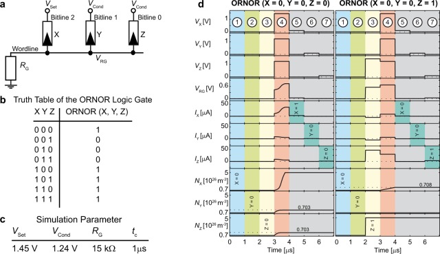
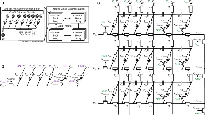
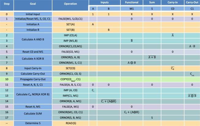
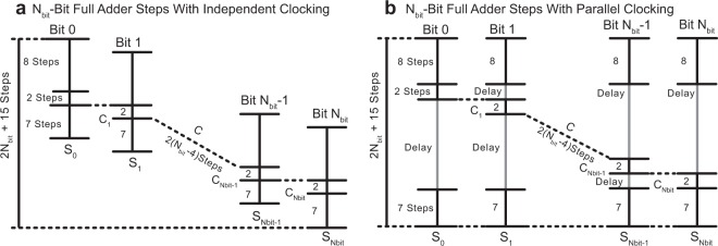
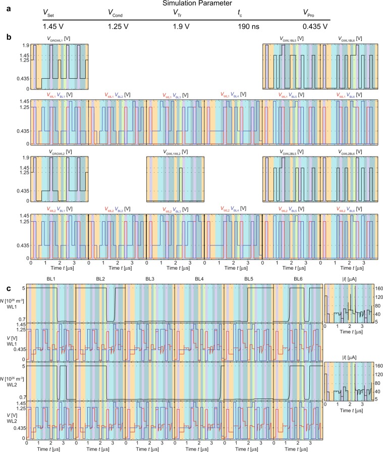
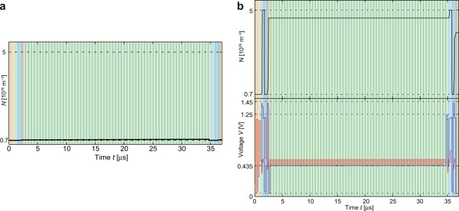
Memristive switches are able to act as both storage and computing elements, which make them an excellent candidate for beyond-CMOS computing. In this paper, multi-input memristive switch logic is proposed, which enables the function X OR (Y NOR Z) to be performed in a single-step with three memristive switches. This ORNOR logic gate increases the capabilities of memristive switches, improving the overall system efficiency of a memristive switch-based computing architecture. Additionally, a computing system architecture and clocking scheme are proposed to further utilize memristive switching for computation. The system architecture is based on a design where multiple computational function blocks are interconnected and controlled by a master clock that synchronizes system data processing and transfer. The clocking steps to perform a full adder with the ORNOR gate are presented along with simulation results using a physics-based model. The full adder function block is integrated into the system architecture to realize a 64-bit full adder, which is also demonstrated through simulation.
忆阻开关既能充当存储元件,又能充当计算元件,这使其成为超越互补金属氧化物半导体(CMOS)计算的理想选择。本文提出了多输入忆阻开关逻辑,它能使“X异或(Y或非Z)”功能通过三个忆阻开关一步实现。这种或非逻辑门增强了忆阻开关的能力,提高了基于忆阻开关的计算架构的整体系统效率。此外,还提出了一种计算系统架构和时钟方案,以进一步利用忆阻开关进行计算。该系统架构基于这样一种设计,即多个计算功能块相互连接,并由一个主时钟控制,该主时钟同步系统数据处理和传输。给出了使用基于物理的模型,用或非门执行一位全加器的时钟步骤以及仿真结果。全加器功能块被集成到系统架构中以实现一个64位全加器,这也通过仿真得到了验证。