State Key Laboratory of Infrared Physics, Key Laboratory of Intelligent Infrared Perception, Shanghai Institute of Technical Physics, Chinese Academy of Sciences, 200083, Shanghai, China.
University of Chinese Academy of Sciences, Chinese Academy of Sciences, 100049, Beijing, China.
Nat Commun. 2019 Oct 11;10(1):4663. doi: 10.1038/s41467-019-12707-3.
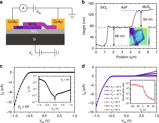
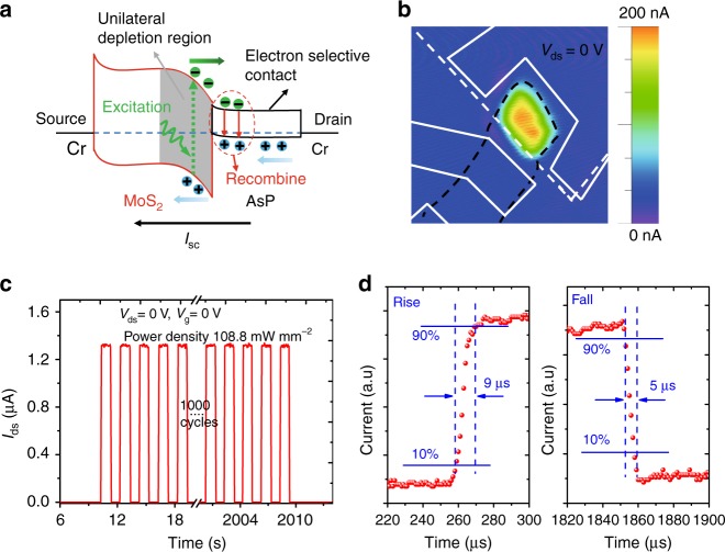
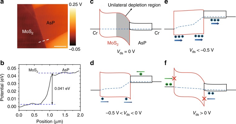
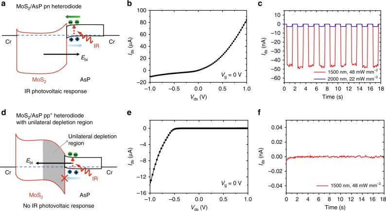
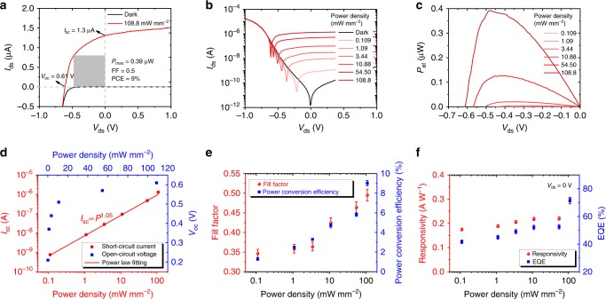
Van der Waals (vdW) heterodiodes based on two-dimensional (2D) materials have shown tremendous potential in photovoltaic detectors and solar cells. However, such 2D photovoltaic devices are limited by low quantum efficiencies due to the severe interface recombination and the inefficient contacts. Here, we report an efficient MoS/AsP vdW hetero-photodiode utilizing a unilateral depletion region band design and a narrow bandgap AsP as an effective carrier selective contact. The unilateral depletion region is verified via both the Fermi level and the infrared response measurements. The device demonstrates a pronounced photovoltaic behavior with a short-circuit current of 1.3 μA and a large open-circuit voltage of 0.61 V under visible light illumination. Especially, a high external quantum efficiency of 71%, a record high power conversion efficiency of 9% and a fast response time of 9 μs are achieved. Our work suggests an effective scheme to design high-performance photovoltaic devices assembled by 2D materials.
基于二维(2D)材料的范德华(vdW)异质二极体在光伏探测器和太阳能电池中显示出巨大的潜力。然而,由于严重的界面复合和低效的接触,这种 2D 光伏器件的量子效率受到限制。在这里,我们报告了一种利用单侧耗尽区能带设计和窄带隙 AsP 作为有效载流子选择接触的高效 MoS/AsP vdW 异质光电二极管。通过费米能级和红外响应测量验证了单侧耗尽区。该器件在可见光照射下表现出明显的光伏行为,短路电流为 1.3μA,开路电压为 0.61V。特别是,实现了 71%的高光外量子效率、创纪录的 9%功率转换效率和 9μs 的快速响应时间。我们的工作为设计由 2D 材料组装的高性能光伏器件提供了一种有效的方案。