• 文献检索
  • 文档翻译
  • 深度研究
  • 学术资讯
  • Suppr Zotero 插件Zotero 插件
  • 邀请有礼
  • 套餐&价格
  • 历史记录
应用&插件
Suppr Zotero 插件Zotero 插件浏览器插件Mac 客户端Windows 客户端微信小程序
定价
高级版会员购买积分包购买API积分包
服务
文献检索文档翻译深度研究API 文档MCP 服务
关于我们
关于 Suppr公司介绍联系我们用户协议隐私条款
关注我们

Suppr 超能文献

核心技术专利:CN118964589B侵权必究
粤ICP备2023148730 号-1Suppr @ 2026

文献检索

告别复杂PubMed语法,用中文像聊天一样搜索,搜遍4000万医学文献。AI智能推荐,让科研检索更轻松。

立即免费搜索

文件翻译

保留排版,准确专业,支持PDF/Word/PPT等文件格式,支持 12+语言互译。

免费翻译文档

深度研究

AI帮你快速写综述,25分钟生成高质量综述,智能提取关键信息,辅助科研写作。

立即免费体验

透明多光谱光电探测器,模拟人类视觉系统。

Transparent multispectral photodetectors mimicking the human visual system.

机构信息

Geballe Laboratory for Advanced Materials, Stanford University, Stanford, CA, USA.

CREOL, The College of Optics and Photonics, University of Central Florida, Orlando, FL, USA.

出版信息

Nat Commun. 2019 Nov 1;10(1):4982. doi: 10.1038/s41467-019-12899-8.

DOI:10.1038/s41467-019-12899-8
PMID:31676782
原文链接:https://pmc.ncbi.nlm.nih.gov/articles/PMC6825164/
Abstract

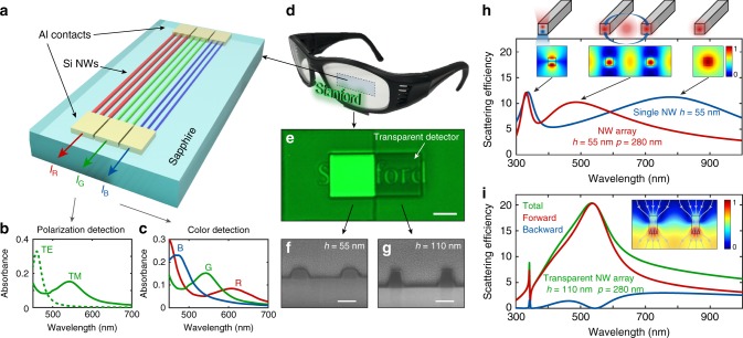
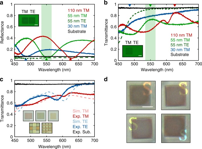
Compact and lightweight photodetection elements play a critical role in the newly emerging augmented reality, wearable and sensing technologies. In these technologies, devices are preferred to be transparent to form an optical interface between a viewer and the outside world. For this reason, it is of great value to create detection platforms that are imperceptible to the human eye directly onto transparent substrates. Semiconductor nanowires (NWs) make ideal photodetectors as their optical resonances enable parsing of the multi-dimensional information carried by light. Unfortunately, these optical resonances also give rise to strong, undesired light scattering. In this work, we illustrate how a new optical resonance arising from the radiative coupling between arrayed silicon NWs can be harnessed to remove reflections from dielectric interfaces while affording spectro-polarimetric detection. The demonstrated transparent photodetector concept opens up promising platforms for transparent substrates as the base for opto-electronic devices and in situ optical measurement systems.

摘要

紧凑型、轻量化的光电探测元件在新兴的增强现实、可穿戴和传感技术中起着至关重要的作用。在这些技术中,人们希望设备是透明的,以便在观察者和外部世界之间形成光学接口。出于这个原因,创造直接在透明衬底上的人眼不可见的检测平台具有重要价值。半导体纳米线 (NWs) 作为光电探测器非常理想,因为它们的光学共振使人们能够解析光所携带的多维信息。不幸的是,这些光学共振也会引起强烈的、不需要的光散射。在这项工作中,我们展示了如何利用阵列硅 NWs 之间的辐射耦合产生的新光学共振来消除介电界面的反射,同时提供光谱偏振检测。所展示的透明光电探测器概念为透明衬底作为光电设备和原位光学测量系统的基础提供了有前途的平台。

https://cdn.ncbi.nlm.nih.gov/pmc/blobs/b594/6825164/a57bacc1cb0b/41467_2019_12899_Fig3_HTML.jpg
https://cdn.ncbi.nlm.nih.gov/pmc/blobs/b594/6825164/6381ff5862f9/41467_2019_12899_Fig1_HTML.jpg
https://cdn.ncbi.nlm.nih.gov/pmc/blobs/b594/6825164/0a5bb0bae28e/41467_2019_12899_Fig2_HTML.jpg
https://cdn.ncbi.nlm.nih.gov/pmc/blobs/b594/6825164/a57bacc1cb0b/41467_2019_12899_Fig3_HTML.jpg
https://cdn.ncbi.nlm.nih.gov/pmc/blobs/b594/6825164/6381ff5862f9/41467_2019_12899_Fig1_HTML.jpg
https://cdn.ncbi.nlm.nih.gov/pmc/blobs/b594/6825164/0a5bb0bae28e/41467_2019_12899_Fig2_HTML.jpg
https://cdn.ncbi.nlm.nih.gov/pmc/blobs/b594/6825164/a57bacc1cb0b/41467_2019_12899_Fig3_HTML.jpg

相似文献

1
Transparent multispectral photodetectors mimicking the human visual system.透明多光谱光电探测器,模拟人类视觉系统。
Nat Commun. 2019 Nov 1;10(1):4982. doi: 10.1038/s41467-019-12899-8.
2
Metal-insulator-semiconductor photodetectors.金属-绝缘体-半导体光电探测器。
Sensors (Basel). 2010;10(10):8797-826. doi: 10.3390/s101008797. Epub 2010 Sep 28.
3
Wafer-scale design of lightweight and transparent electronics that wraps around hairs.晶圆级设计的轻质透明电子器件,可缠绕在毛发上。
Nat Commun. 2014;5:2982. doi: 10.1038/ncomms3982.
4
Vertical chip-to-chip coupling between silicon photonic integrated circuits using cantilever couplers.使用悬臂耦合器实现硅光子集成电路之间的垂直芯片间耦合。
Opt Express. 2011 Feb 28;19(5):4722-7. doi: 10.1364/OE.19.004722.
5
Optical coupling of deep-subwavelength semiconductor nanowires.深亚波长半导体纳米线的光耦合。
Nano Lett. 2011 Apr 13;11(4):1463-8. doi: 10.1021/nl1040429. Epub 2011 Mar 28.
6
Subwavelength angle-sensing photodetectors inspired by directional hearing in small animals.受小动物声向性听觉启发的亚波长角度感应光电探测器。
Nat Nanotechnol. 2018 Dec;13(12):1143-1147. doi: 10.1038/s41565-018-0278-9. Epub 2018 Oct 29.
7
Tuning light absorption in core/shell silicon nanowire photovoltaic devices through morphological design.通过形态设计调节核壳硅纳米线光伏器件的光吸收。
Nano Lett. 2012 Sep 12;12(9):4971-6. doi: 10.1021/nl302578z. Epub 2012 Aug 21.
8
Multi-channel silicon photonic receiver based on ring-resonators.基于环形谐振器的多通道硅光子接收器。
Opt Express. 2010 Jun 21;18(13):13510-5. doi: 10.1364/OE.18.013510.
9
All-optical active switching in individual semiconductor nanowires.单个半导体纳米线中的全光学有源开关。
Nat Nanotechnol. 2012 Oct;7(10):640-5. doi: 10.1038/nnano.2012.144. Epub 2012 Sep 2.
10
Microscopic sensors using optical wireless integrated circuits.使用光学无线集成电路的微观传感器。
Proc Natl Acad Sci U S A. 2020 Apr 28;117(17):9173-9179. doi: 10.1073/pnas.1919677117. Epub 2020 Apr 17.

引用本文的文献

1
Fully degradable, transparent, and flexible photodetectors using ZnO nanowires and PEDOT:PSS based nanofibres.使用氧化锌纳米线和基于聚(3,4-乙撑二氧噻吩):聚苯乙烯磺酸盐的纳米纤维制成的完全可降解、透明且灵活的光电探测器。
Npj Flex Electron. 2025;9(1):22. doi: 10.1038/s41528-025-00385-9. Epub 2025 Mar 10.
2
A Bias-Tunable Multispectral Photodetector Based on a GaN/TeSe Homo-Type Heterojunction with a Unidirectional Barrier.基于具有单向势垒的GaN/TeSe同质结的偏置可调谐多光谱光电探测器。
Adv Sci (Weinh). 2025 May;12(17):e2417428. doi: 10.1002/advs.202417428. Epub 2025 Mar 7.
3
3D Light-Direction Sensor Based on Segmented Concentric Nanorings Combined with Deep Learning.

本文引用的文献

1
Subwavelength angle-sensing photodetectors inspired by directional hearing in small animals.受小动物声向性听觉启发的亚波长角度感应光电探测器。
Nat Nanotechnol. 2018 Dec;13(12):1143-1147. doi: 10.1038/s41565-018-0278-9. Epub 2018 Oct 29.
2
Generalized Kerker effects in nanophotonics and meta-optics [Invited].纳米光子学和超光学中的广义克尔效应[特邀报告]
Opt Express. 2018 May 14;26(10):13085-13105. doi: 10.1364/OE.26.013085.
3
Metasurface Mirrors for External Control of Mie Resonances.用于米氏共振外部控制的亚表面镜。
基于分段同心纳米环与深度学习相结合的3D光方向传感器
Micromachines (Basel). 2024 Sep 30;15(10):1219. doi: 10.3390/mi15101219.
4
Centrifugal Inertia-Induced Directional Alignment of AgNW Network for Preparing Transparent Electromagnetic Interference Shielding Films with Joule Heating Ability.用于制备具有焦耳热能力的透明电磁干扰屏蔽膜的银纳米线网络的离心惯性诱导定向排列
Adv Sci (Weinh). 2024 Oct;11(38):e2406758. doi: 10.1002/advs.202406758. Epub 2024 Aug 8.
5
Temperature-Dependent Excitonic Light Manipulation with Atomically Thin Optical Elements.利用原子级薄光学元件实现温度依赖的激子光操控
Nano Lett. 2024 May 29;24(21):6240-6246. doi: 10.1021/acs.nanolett.4c00694. Epub 2024 Apr 5.
6
Localised surface plasmon resonance inducing cooperative Jahn-Teller effect for crystal phase-change in a nanocrystal.局域表面等离子体共振诱导纳米晶体中晶体相变的协同 Jahn-Teller 效应
Nat Commun. 2023 Jul 31;14(1):4471. doi: 10.1038/s41467-023-40153-9.
7
Improving Photosensitivity and Transparency in Organic Phototransistor with Blending Insulating Polymers.通过混合绝缘聚合物提高有机光电晶体管的光敏性和透明度
Micromachines (Basel). 2023 Mar 8;14(3):620. doi: 10.3390/mi14030620.
8
Miniaturizing color-sensitive photodetectors via hybrid nanoantennas toward submicrometer dimensions.通过混合纳米天线将颜色敏感光探测器微型化至亚微米尺寸。
Sci Adv. 2022 Nov 25;8(47):eadd3868. doi: 10.1126/sciadv.add3868. Epub 2022 Nov 23.
9
Anisotropic charge trapping in phototransistors unlocks ultrasensitive polarimetry for bionic navigation.各向异性电荷俘获在光晶体管中解锁了用于仿生导航的超灵敏偏振测量。
Nat Commun. 2022 Nov 4;13(1):6629. doi: 10.1038/s41467-022-34421-3.
10
Coupled Multiphysics Modelling of Sensors for Chemical, Biomedical, and Environmental Applications with Focus on Smart Materials and Low-Dimensional Nanostructures.用于化学、生物医学和环境应用的传感器的耦合多物理场建模,重点关注智能材料和低维纳米结构。
Chemosensors (Basel). 2022 Apr 25;10(5):157. doi: 10.3390/chemosensors10050157. eCollection 2022 May.
Nano Lett. 2018 Jun 13;18(6):3857-3864. doi: 10.1021/acs.nanolett.8b01148. Epub 2018 May 25.
4
Anti-Hermitian photodetector facilitating efficient subwavelength photon sorting.实现高效亚波长光子分选的反厄米光探测器。
Nat Commun. 2018 Jan 22;9(1):316. doi: 10.1038/s41467-017-02496-y.
5
Purcell effect for active tuning of light scattering from semiconductor optical antennas.利用 Purcell 效应主动调谐半导体光天线的光散射。
Science. 2017 Dec 15;358(6369):1407-1410. doi: 10.1126/science.aao5371.
6
Visible Wavelength Color Filters Using Dielectric Subwavelength Gratings for Backside-Illuminated CMOS Image Sensor Technologies.基于介质亚波长光栅的背面照明 CMOS 图像传感器用可见波长滤色片。
Nano Lett. 2017 May 10;17(5):3159-3164. doi: 10.1021/acs.nanolett.7b00636. Epub 2017 Apr 13.
7
Optically resonant dielectric nanostructures.光学共振介质纳米结构。
Science. 2016 Nov 18;354(6314). doi: 10.1126/science.aag2472.
8
Experimental Demonstration of Adaptive Infrared Multispectral Imaging using Plasmonic Filter Array.利用等离子体滤波阵列进行自适应红外多光谱成像的实验演示。
Sci Rep. 2016 Oct 10;6:34876. doi: 10.1038/srep34876.
9
Nanophotonic Image Sensors.纳米光子图像传感器
Small. 2016 Sep;12(36):4922-4935. doi: 10.1002/smll.201600528. Epub 2016 May 30.
10
Color-selective and CMOS-compatible photodetection based on aluminum plasmonics.基于铝等离子体光学的颜色选择性和 CMOS 兼容光电探测。
Adv Mater. 2014 Sep;26(36):6318-23. doi: 10.1002/adma.201401168. Epub 2014 Aug 5.