• 文献检索
  • 文档翻译
  • 深度研究
  • 学术资讯
  • Suppr Zotero 插件Zotero 插件
  • 邀请有礼
  • 套餐&价格
  • 历史记录
应用&插件
Suppr Zotero 插件Zotero 插件浏览器插件Mac 客户端Windows 客户端微信小程序
定价
高级版会员购买积分包购买API积分包
服务
文献检索文档翻译深度研究API 文档MCP 服务
关于我们
关于 Suppr公司介绍联系我们用户协议隐私条款
关注我们

Suppr 超能文献

核心技术专利:CN118964589B侵权必究
粤ICP备2023148730 号-1Suppr @ 2026

文献检索

告别复杂PubMed语法,用中文像聊天一样搜索,搜遍4000万医学文献。AI智能推荐,让科研检索更轻松。

立即免费搜索

文件翻译

保留排版,准确专业,支持PDF/Word/PPT等文件格式,支持 12+语言互译。

免费翻译文档

深度研究

AI帮你快速写综述,25分钟生成高质量综述,智能提取关键信息,辅助科研写作。

立即免费体验

用于超薄MoS薄片电输运和场发射表征的纳米尖端接触

Nanotip Contacts for Electric Transport and Field Emission Characterization of Ultrathin MoS Flakes.

作者信息

Iemmo Laura, Urban Francesca, Giubileo Filippo, Passacantando Maurizio, Di Bartolomeo Antonio

机构信息

Department of Physics 'E.R.Caianello', University of Salerno, Via Giovanni Paolo II, 132-84084 Fisciano (SA), Italy.

CNR-SPIN Institute, Via Giovanni Paolo II, 132-84084 Fisciano (SA), Italy.

出版信息

Nanomaterials (Basel). 2020 Jan 4;10(1):106. doi: 10.3390/nano10010106.

DOI:10.3390/nano10010106
PMID:31947985
原文链接:https://pmc.ncbi.nlm.nih.gov/articles/PMC7023401/
Abstract

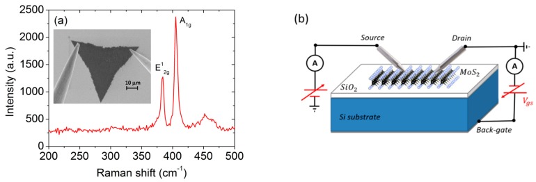
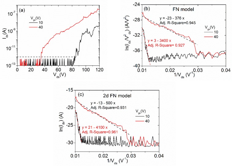
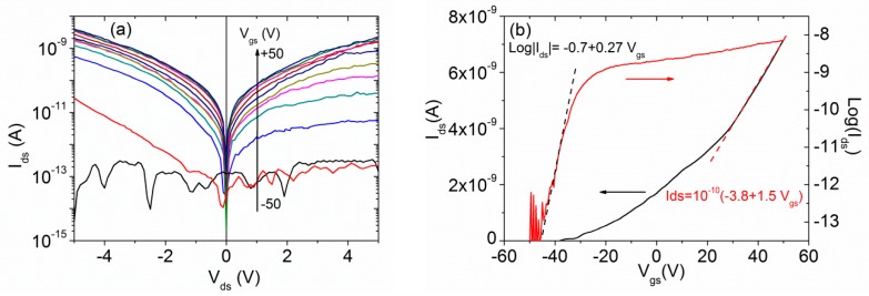
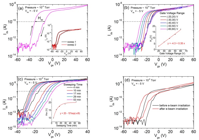
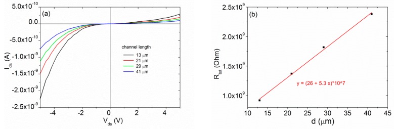
We report a facile approach based on piezoelectric-driven nanotips inside a scanning electron microscope to contact and electrically characterize ultrathin MoS2 (molybdenum disulfide) flakes on a SiO2/Si (silicon dioxide/silicon) substrate. We apply such a method to analyze the electric transport and field emission properties of chemical vapor deposition-synthesized monolayer MoS, used as the channel of back-gate field effect transistors. We study the effects of the gate-voltage range and sweeping time on the channel current and on its hysteretic behavior. We observe that the conduction of the MoS channel is affected by trap states. Moreover, we report a gate-controlled field emission current from the edge part of the MoS flake, evidencing a field enhancement factor of approximately 200 and a turn-on field of approximately   40   V / μ m at a cathode-anode separation distance of 900   nm .

摘要

我们报告了一种基于扫描电子显微镜内压电驱动纳米尖端的简便方法,用于接触并电学表征SiO₂/Si(二氧化硅/硅)衬底上的超薄二硫化钼(MoS₂)薄片。我们应用这种方法来分析用作背栅场效应晶体管沟道的化学气相沉积合成单层MoS₂的电输运和场发射特性。我们研究了栅极电压范围和扫描时间对沟道电流及其滞后行为的影响。我们观察到MoS₂沟道的传导受陷阱态影响。此外,我们报告了来自MoS₂薄片边缘部分的栅极控制场发射电流,在阴极 - 阳极分离距离为900 nm时,场增强因子约为200,开启场约为40 V /μm。

https://cdn.ncbi.nlm.nih.gov/pmc/blobs/86de/7023401/d67114787e2b/nanomaterials-10-00106-g005.jpg
https://cdn.ncbi.nlm.nih.gov/pmc/blobs/86de/7023401/1106004161b1/nanomaterials-10-00106-g001.jpg
https://cdn.ncbi.nlm.nih.gov/pmc/blobs/86de/7023401/39941c388858/nanomaterials-10-00106-g002.jpg
https://cdn.ncbi.nlm.nih.gov/pmc/blobs/86de/7023401/c1efb53d93a4/nanomaterials-10-00106-g003.jpg
https://cdn.ncbi.nlm.nih.gov/pmc/blobs/86de/7023401/c5666eeeffbb/nanomaterials-10-00106-g004.jpg
https://cdn.ncbi.nlm.nih.gov/pmc/blobs/86de/7023401/d67114787e2b/nanomaterials-10-00106-g005.jpg

相似文献

1
Nanotip Contacts for Electric Transport and Field Emission Characterization of Ultrathin MoS Flakes.用于超薄MoS薄片电输运和场发射表征的纳米尖端接触
Nanomaterials (Basel). 2020 Jan 4;10(1):106. doi: 10.3390/nano10010106.
2
Transport and Field Emission Properties of MoS₂ Bilayers.二硫化钼双层膜的输运和场发射特性
Nanomaterials (Basel). 2018 Mar 8;8(3):151. doi: 10.3390/nano8030151.
3
Probing the Field-Effect Transistor with Monolayer MoS Prepared by APCVD.用常压化学气相沉积法制备的单层二硫化钼探测场效应晶体管。
Nanomaterials (Basel). 2019 Aug 27;9(9):1209. doi: 10.3390/nano9091209.
4
Strain-Gated Field Effect Transistor of a MoS2-ZnO 2D-1D Hybrid Structure.MoS2-ZnO 二维-一维混合结构的应变门场效应晶体管。
ACS Nano. 2016 Jan 26;10(1):1546-51. doi: 10.1021/acsnano.5b07121. Epub 2015 Dec 29.
5
Monolayer MoS field effect transistor with low Schottky barrier height with ferromagnetic metal contacts.具有与铁磁金属接触的低肖特基势垒高度的单层MoS场效应晶体管。
Sci Rep. 2019 Nov 19;9(1):17032. doi: 10.1038/s41598-019-53367-z.
6
2D MoS Field-Effect Transistors with an Electron Beam Gate.具有电子束栅极的二维二硫化钼场效应晶体管。
ACS Nano. 2020 Jun 23;14(6):7389-7397. doi: 10.1021/acsnano.0c02908. Epub 2020 May 14.
7
Statistical study of deep submicron dual-gated field-effect transistors on monolayer chemical vapor deposition molybdenum disulfide films.深亚微米双层门场效应晶体管在单层化学气相沉积二硫化钼薄膜上的统计研究。
Nano Lett. 2013 Jun 12;13(6):2640-6. doi: 10.1021/nl400778q. Epub 2013 May 20.
8
Strain Gated Bilayer Molybdenum Disulfide Field Effect Transistor with Edge Contacts.应变门控双层二硫化钼场效应晶体管的边缘接触
Sci Rep. 2017 Feb 10;7:41593. doi: 10.1038/srep41593.
9
Charge-Ferroelectric Transition in Ultrathin Na Bi Ti O Flakes Probed via a Dual-Gated Full van der Waals Transistor.通过双栅全范德瓦尔斯晶体管探测超薄NaBiTiO薄片中的电荷-铁电转变
Adv Mater. 2020 Dec;32(49):e2004813. doi: 10.1002/adma.202004813. Epub 2020 Nov 3.
10
Probing Interface Defects in Top-Gated MoS Transistors with Impedance Spectroscopy.用阻抗谱研究顶栅 MoS 晶体管中的界面缺陷。
ACS Appl Mater Interfaces. 2017 Jul 19;9(28):24348-24356. doi: 10.1021/acsami.7b06204. Epub 2017 Jul 6.

引用本文的文献

1
Current Advances in Nanoelectronics, Nanosensors, and Devices.纳米电子学、纳米传感器及器件的当前进展
Nanomaterials (Basel). 2024 Nov 4;14(21):1771. doi: 10.3390/nano14211771.
2
Nanotubes from Transition Metal Dichalcogenides: Recent Progress in the Synthesis, Characterization and Electrooptical Properties.过渡金属二硫属化物纳米管:合成、表征及电光性质的最新进展
Small. 2025 Jul;21(28):e2400503. doi: 10.1002/smll.202400503. Epub 2024 Jul 2.
3
Cold Cathodes with Two-Dimensional van der Waals Materials.具有二维范德华材料的冷阴极

本文引用的文献

1
A WSe vertical field emission transistor.一个 WSe 垂直场发射晶体管。
Nanoscale. 2019 Jan 23;11(4):1538-1548. doi: 10.1039/c8nr09068h.
2
Advances in MoS-Based Field Effect Transistors (FETs).基于二硫化钼的场效应晶体管(FET)的进展。
Nanomicro Lett. 2015;7(3):203-218. doi: 10.1007/s40820-015-0034-8. Epub 2015 Feb 13.
3
Environmental Effects on the Electrical Characteristics of Back-Gated WSe₂ Field-Effect Transistors.环境对背栅WSe₂场效应晶体管电学特性的影响
Nanomaterials (Basel). 2023 Aug 28;13(17):2437. doi: 10.3390/nano13172437.
4
Tabletop Fabrication of High-Performance MoS Field-Effect Transistors.高性能MoS场效应晶体管的桌面制造
ACS Omega. 2022 Jun 10;7(24):21220-21224. doi: 10.1021/acsomega.2c02188. eCollection 2022 Jun 21.
5
Superconducting- and Graphene-Based Devices.基于超导和石墨烯的器件
Nanomaterials (Basel). 2022 Jun 15;12(12):2055. doi: 10.3390/nano12122055.
6
Emerging 2D Materials and Their Van Der Waals Heterostructures.新兴二维材料及其范德华异质结构
Nanomaterials (Basel). 2020 Mar 22;10(3):579. doi: 10.3390/nano10030579.
7
Observation of 2D Conduction in Ultrathin Germanium Arsenide Field-Effect Transistors.超薄砷化锗场效应晶体管中二维传导的观测
ACS Appl Mater Interfaces. 2020 Mar 18;12(11):12998-13004. doi: 10.1021/acsami.0c00348. Epub 2020 Mar 9.
Nanomaterials (Basel). 2018 Nov 3;8(11):901. doi: 10.3390/nano8110901.
4
Transport and Field Emission Properties of MoS₂ Bilayers.二硫化钼双层膜的输运和场发射特性
Nanomaterials (Basel). 2018 Mar 8;8(3):151. doi: 10.3390/nano8030151.
5
Graphene enhanced field emission from InP nanocrystals.石墨烯增强的 InP 纳米晶体场发射。
Nanotechnology. 2017 Dec 8;28(49):495705. doi: 10.1088/1361-6528/aa96e6.
6
Field Emission from Self-Catalyzed GaAs Nanowires.自催化生长的砷化镓纳米线的场发射
Nanomaterials (Basel). 2017 Sep 16;7(9):275. doi: 10.3390/nano7090275.
7
Observation of field emission from GeSn nanoparticles epitaxially grown on silicon nanopillar arrays.观察锗锡纳米粒子在硅纳米柱阵列上外延生长的场发射。
Nanotechnology. 2016 Dec 2;27(48):485707. doi: 10.1088/0957-4484/27/48/485707. Epub 2016 Nov 2.
8
Interfacial Properties of Monolayer and Bilayer MoS2 Contacts with Metals: Beyond the Energy Band Calculations.单层和双层二硫化钼与金属接触的界面特性:超越能带计算
Sci Rep. 2016 Mar 1;6:21786. doi: 10.1038/srep21786.
9
Low voltage and high ON/OFF ratio field-effect transistors based on CVD MoS2 and ultra high-k gate dielectric PZT.基于 CVD MoS2 和超高介电常数 PZT 的低电压、高导通/关断比场效应晶体管。
Nanoscale. 2015 May 21;7(19):8695-700. doi: 10.1039/c5nr01072a.
10
Nanodiamonds for field emission: state of the art.用于场发射的纳米金刚石:现状
Nanoscale. 2015 Mar 12;7(12):5094-114. doi: 10.1039/c4nr07171a.