• 文献检索
  • 文档翻译
  • 深度研究
  • 学术资讯
  • Suppr Zotero 插件Zotero 插件
  • 邀请有礼
  • 套餐&价格
  • 历史记录
应用&插件
Suppr Zotero 插件Zotero 插件浏览器插件Mac 客户端Windows 客户端微信小程序
定价
高级版会员购买积分包购买API积分包
服务
文献检索文档翻译深度研究API 文档MCP 服务
关于我们
关于 Suppr公司介绍联系我们用户协议隐私条款
关注我们

Suppr 超能文献

核心技术专利:CN118964589B侵权必究
粤ICP备2023148730 号-1Suppr @ 2026

文献检索

告别复杂PubMed语法,用中文像聊天一样搜索,搜遍4000万医学文献。AI智能推荐,让科研检索更轻松。

立即免费搜索

文件翻译

保留排版,准确专业,支持PDF/Word/PPT等文件格式,支持 12+语言互译。

免费翻译文档

深度研究

AI帮你快速写综述,25分钟生成高质量综述,智能提取关键信息,辅助科研写作。

立即免费体验

利用双功能聚合物薄膜实现范德华异质结构的多功能构建。

Versatile construction of van der Waals heterostructures using a dual-function polymeric film.

作者信息

Huang Zhujun, Alharbi Abdullah, Mayer William, Cuniberto Edoardo, Taniguchi Takashi, Watanabe Kenji, Shabani Javad, Shahrjerdi Davood

机构信息

Electrical and Computer Engineering, New York University, Brooklyn, NY, 11201, USA.

King Abdulaziz City for Science and Technology, Riyadh, 11442, Saudi Arabia.

出版信息

Nat Commun. 2020 Jun 15;11(1):3029. doi: 10.1038/s41467-020-16817-1.

DOI:10.1038/s41467-020-16817-1
PMID:32541673
原文链接:https://pmc.ncbi.nlm.nih.gov/articles/PMC7295972/
Abstract

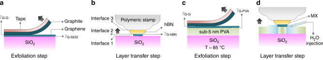
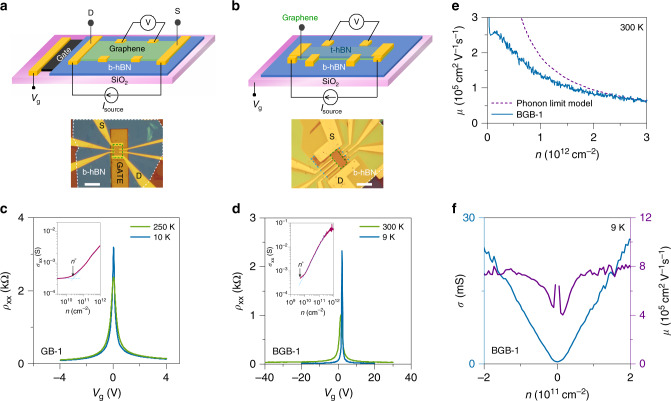
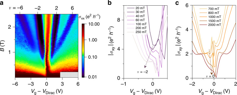
The proliferation of van der Waals (vdW) heterostructures formed by stacking layered materials can accelerate scientific and technological advances. Here, we report a strategy for constructing vdW heterostructures through the interface engineering of the exfoliation substrate using a sub-5 nm polymeric film. Our construction method has two main features that distinguish it from existing techniques. First is the consistency of its exfoliation process in increasing the yield and in producing large (>10,000 μm) monolayer graphene. Second is the applicability of its layer transfer process to different layered materials without requiring a specialized stamp-a feature useful for generalizing the assembly process. We demonstrate vdW graphene devices with peak carrier mobility of 200,000 and 800,000 cm V s at room temperature and 9 K, respectively. The simplicity of our construction method and its versatility to different layered materials may open doors for automating the fabrication process of vdW heterostructures.

摘要

通过堆叠层状材料形成的范德华(vdW)异质结构的激增可以加速科技进步。在此,我们报告了一种使用亚5纳米聚合物薄膜通过剥离衬底的界面工程构建vdW异质结构的策略。我们的构建方法有两个主要特征使其有别于现有技术。首先是其在提高产量和生产大面积(>10,000μm)单层石墨烯方面剥离过程的一致性。其次是其层转移过程适用于不同的层状材料,而无需专门的印章——这一特性有助于推广组装过程。我们展示了在室温下峰值载流子迁移率为200,000 cm² V⁻¹ s⁻¹、在9 K时为800,000 cm² V⁻¹ s⁻¹的vdW石墨烯器件。我们构建方法的简单性及其对不同层状材料的通用性可能为vdW异质结构的自动化制造过程打开大门。

https://cdn.ncbi.nlm.nih.gov/pmc/blobs/0404/7295972/866ce132a08f/41467_2020_16817_Fig6_HTML.jpg
https://cdn.ncbi.nlm.nih.gov/pmc/blobs/0404/7295972/3760c38ea152/41467_2020_16817_Fig1_HTML.jpg
https://cdn.ncbi.nlm.nih.gov/pmc/blobs/0404/7295972/6d99412496f4/41467_2020_16817_Fig2_HTML.jpg
https://cdn.ncbi.nlm.nih.gov/pmc/blobs/0404/7295972/9c77c750f655/41467_2020_16817_Fig3_HTML.jpg
https://cdn.ncbi.nlm.nih.gov/pmc/blobs/0404/7295972/add4d72d438f/41467_2020_16817_Fig4_HTML.jpg
https://cdn.ncbi.nlm.nih.gov/pmc/blobs/0404/7295972/996cc8fa9b28/41467_2020_16817_Fig5_HTML.jpg
https://cdn.ncbi.nlm.nih.gov/pmc/blobs/0404/7295972/866ce132a08f/41467_2020_16817_Fig6_HTML.jpg

相似文献

1
Versatile construction of van der Waals heterostructures using a dual-function polymeric film.利用双功能聚合物薄膜实现范德华异质结构的多功能构建。
Nat Commun. 2020 Jun 15;11(1):3029. doi: 10.1038/s41467-020-16817-1.
2
van der Waals Layered Materials: Opportunities and Challenges.范德华层状材料:机遇与挑战。
ACS Nano. 2017 Dec 26;11(12):11803-11830. doi: 10.1021/acsnano.7b07436. Epub 2017 Dec 13.
3
Large-Area Synthesis of Ferromagnetic Fe GeTe /Graphene van der Waals Heterostructures with Curie Temperature above Room Temperature.大面积合成居里温度高于室温的铁磁体Fe₃GeTe₂/石墨烯范德华异质结构
Small. 2023 Sep;19(39):e2302387. doi: 10.1002/smll.202302387. Epub 2023 May 25.
4
Synthesis of hexagonal boron nitride heterostructures for 2D van der Waals electronics.六方氮化硼异质结构的合成及其在二维范德华电子学中的应用。
Chem Soc Rev. 2018 Aug 13;47(16):6342-6369. doi: 10.1039/c8cs00450a.
5
Synthesis of AAB-Stacked Single-Crystal Graphene/hBN/Graphene Trilayer van der Waals Heterostructures by In Situ CVD.通过原位化学气相沉积法合成AAB堆叠的单晶石墨烯/hBN/石墨烯三层范德华异质结构
Adv Sci (Weinh). 2022 Jul;9(21):e2201324. doi: 10.1002/advs.202201324. Epub 2022 May 26.
6
Constructing van der Waals heterostructures by dry-transfer assembly for novel optoelectronic device.通过干转移组装构建用于新型光电器件的范德华异质结构。
Nanotechnology. 2022 Aug 30;33(46). doi: 10.1088/1361-6528/ac5f96.
7
Bubble-Free Transfer Technique for High-Quality Graphene/Hexagonal Boron Nitride van der Waals Heterostructures.用于高质量石墨烯/六方氮化硼范德华异质结构的无气泡转移技术
ACS Appl Mater Interfaces. 2020 Feb 19;12(7):8533-8538. doi: 10.1021/acsami.9b19191. Epub 2020 Feb 6.
8
BiO/BiVO@graphene oxide van der Waals heterostructures with enhanced photocatalytic activity toward oxygen generation.具有增强的光催化产氧活性的BiO/BiVO@氧化石墨烯范德华异质结构
J Colloid Interface Sci. 2021 Jul;593:196-203. doi: 10.1016/j.jcis.2021.02.079. Epub 2021 Mar 9.
9
Wafer-Scale van der Waals Heterostructures with Ultraclean Interfaces via the Aid of Viscoelastic Polymer.借助粘弹性聚合物实现具有超清洁界面的晶圆级范德华异质结构
ACS Appl Mater Interfaces. 2019 Jan 9;11(1):1579-1586. doi: 10.1021/acsami.8b16261. Epub 2018 Dec 21.
10
Enhanced Photoluminescence of Multiple Two-Dimensional van der Waals Heterostructures Fabricated by Layer-by-Layer Oxidation of MoS.通过对二硫化钼进行逐层氧化制备的多种二维范德华异质结构的增强光致发光
ACS Appl Mater Interfaces. 2021 Jan 13;13(1):1245-1252. doi: 10.1021/acsami.0c18364. Epub 2020 Dec 23.

引用本文的文献

1
Van der Waals Heterostructures for Photoelectric, Memory, and Neural Network Applications.用于光电、记忆和神经网络应用的范德华异质结构
Small Sci. 2024 Feb 14;4(4):2300213. doi: 10.1002/smsc.202300213. eCollection 2024 Apr.
2
Synthetic Band Structure Engineering of Graphene Using Block Copolymer-Templated Dielectric Superlattices.利用嵌段共聚物模板化介电超晶格对石墨烯进行合成能带结构工程
ACS Nano. 2025 Mar 18;19(10):9885-9895. doi: 10.1021/acsnano.4c14500. Epub 2025 Mar 6.
3
Mechanical properties of freestanding few-layer graphene/boron nitride/polymer heterostacks investigated with local and non-local techniques.

本文引用的文献

1
Electron Tunneling through Boron Nitride Confirms Marcus-Hush Theory Predictions for Ultramicroelectrodes.电子隧穿氮化硼证实了Marcus-Hush理论对超微电极的预测。
ACS Nano. 2020 Jan 28;14(1):993-1002. doi: 10.1021/acsnano.9b08308. Epub 2019 Dec 17.
2
Direct observation of valley-coupled topological current in MoS.直接观测二硫化钼中的谷耦合拓扑电流。
Sci Adv. 2019 Apr 19;5(4):eaau6478. doi: 10.1126/sciadv.aau6478. eCollection 2019 Apr.
3
Cleaning interfaces in layered materials heterostructures.清洁层状材料异质结构的界面。
采用局部和非局部技术研究独立式少层石墨烯/氮化硼/聚合物异质堆叠结构的力学性能。
Nanoscale Adv. 2024 Sep 26;6(22):5727-34. doi: 10.1039/d4na00514g.
4
Characterizing Defects Inside Hexagonal Boron Nitride Using Random Telegraph Signals in van der Waals 2D Transistors.利用范德华二维晶体管中的随机电报信号表征六方氮化硼内部的缺陷
ACS Nano. 2024 Oct 22;18(42):28700-28711. doi: 10.1021/acsnano.4c06929. Epub 2024 Sep 28.
5
Viscous fingering instabilities in spontaneously formed blisters of MoS multilayers.二硫化钼多层膜自发形成的水泡中的粘性指进不稳定性
Nanoscale Adv. 2023 Oct 30;5(23):6617-6625. doi: 10.1039/d3na00563a. eCollection 2023 Nov 21.
6
Layer-Structured Anisotropic Metal Chalcogenides: Recent Advances in Synthesis, Modulation, and Applications.层状结构的金属硫属化物:在合成、调控及应用方面的最新进展
Chem Rev. 2023 Apr 12;123(7):3329-3442. doi: 10.1021/acs.chemrev.2c00455. Epub 2023 Jan 31.
7
The Magnetic Genome of Two-Dimensional van der Waals Materials.二维范德华材料的磁基因组。
ACS Nano. 2022 May 24;16(5):6960-7079. doi: 10.1021/acsnano.1c09150. Epub 2022 Apr 20.
8
Reconfigurable electronics by disassembling and reassembling van der Waals heterostructures.通过拆解和重新组装范德华异质结构实现的可重构电子器件。
Nat Commun. 2021 Mar 23;12(1):1825. doi: 10.1038/s41467-021-22118-y.
Nat Commun. 2018 Dec 19;9(1):5387. doi: 10.1038/s41467-018-07558-3.
4
Heterointerface effects in the electrointercalation of van der Waals heterostructures.范德华异质结构电嵌入中的异质界面效应。
Nature. 2018 Jun;558(7710):425-429. doi: 10.1038/s41586-018-0205-0. Epub 2018 Jun 20.
5
Observation of the quantum valley Hall state in ballistic graphene superlattices.弹道石墨烯超晶格中量子谷霍尔态的观测
Sci Adv. 2018 May 18;4(5):eaaq0194. doi: 10.1126/sciadv.aaq0194. eCollection 2018 May.
6
Tunable Γ-K Valley Populations in Hole-Doped Trilayer WSe_{2}.掺杂三层 WSe_{2}中的可调 Γ-K 谷载流子。
Phys Rev Lett. 2018 Mar 9;120(10):107703. doi: 10.1103/PhysRevLett.120.107703.
7
Correlated insulator behaviour at half-filling in magic-angle graphene superlattices.在魔角石墨烯超晶格中半填充时的关联绝缘行为。
Nature. 2018 Apr 5;556(7699):80-84. doi: 10.1038/nature26154. Epub 2018 Mar 5.
8
Unconventional superconductivity in magic-angle graphene superlattices.魔角石墨烯超晶格中的非常规超导性。
Nature. 2018 Apr 5;556(7699):43-50. doi: 10.1038/nature26160. Epub 2018 Mar 5.
9
Via Method for Lithography Free Contact and Preservation of 2D Materials.无光刻接触和二维材料保存方法。
Nano Lett. 2018 Feb 14;18(2):1416-1420. doi: 10.1021/acs.nanolett.7b05161. Epub 2018 Feb 5.
10
Layer-by-layer assembly of two-dimensional materials into wafer-scale heterostructures.二维材料的逐层组装成晶圆级异质结。
Nature. 2017 Oct 12;550(7675):229-233. doi: 10.1038/nature23905. Epub 2017 Sep 20.