Colin Jonathan, Jamnig Andreas, Furgeaud Clarisse, Michel Anny, Pliatsikas Nikolaos, Sarakinos Kostas, Abadias Gregory
Institut Pprime, UPR 3346, CNRS-Université de Poitiers-ENSMA, 11 Boulevard Marie et Pierre Curie, TSA 41123, CEDEX 9, 86073 Poitiers, France.
Nanoscale Engineering Division, Department of Physics, Chemistry and Biology, Linköping University, SE 581 83 Linköping, Sweden.
Nanomaterials (Basel). 2020 Nov 9;10(11):2225. doi: 10.3390/nano10112225.
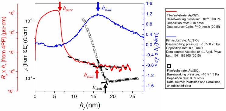
Continued downscaling of functional layers for key enabling devices has prompted the development of characterization tools to probe and dynamically control thin film formation stages and ensure the desired film morphology and functionalities in terms of, e.g., layer surface smoothness or electrical properties. In this work, we review the combined use of in situ and real-time optical (wafer curvature, spectroscopic ellipsometry) and electrical probes for gaining insights into the early growth stages of magnetron-sputter-deposited films. Data are reported for a large variety of metals characterized by different atomic mobilities and interface reactivities. For fcc noble-metal films (Ag, Cu, Pd) exhibiting a pronounced three-dimensional growth on weakly-interacting substrates (SiO, amorphous carbon (a-C)), wafer curvature, spectroscopic ellipsometry, and resistivity techniques are shown to be complementary in studying the morphological evolution of discontinuous layers, and determining the percolation threshold and the onset of continuous film formation. The influence of growth kinetics (in terms of intrinsic atomic mobility, substrate temperature, deposition rate, deposition flux temporal profile) and the effect of deposited energy (through changes in working pressure or bias voltage) on the various morphological transition thicknesses is critically examined. For bcc transition metals, like Fe and Mo deposited on a-Si, in situ and real-time growth monitoring data exhibit transient features at a critical layer thickness of ~2 nm, which is a fingerprint of an interface-mediated crystalline-to-amorphous phase transition, while such behavior is not observed for Ta films that crystallize into their metastable tetragonal β-Ta allotropic phase. The potential of optical and electrical diagnostic tools is also explored to reveal complex interfacial reactions and their effect on growth of Pd films on a-Si or a-Ge interlayers. For all case studies presented in the article, in situ data are complemented with and benchmarked against ex situ structural and morphological analyses.
关键使能器件功能层的持续缩小规模,促使了表征工具的发展,以探测和动态控制薄膜形成阶段,并确保在例如层表面平整度或电学性能方面具有所需的薄膜形态和功能。在这项工作中,我们回顾了原位和实时光学(晶圆曲率、光谱椭偏仪)以及电学探针的联合使用,以深入了解磁控溅射沉积薄膜的早期生长阶段。报告了以不同原子迁移率和界面反应性为特征的多种金属的数据。对于在弱相互作用衬底(SiO、非晶碳(a-C))上呈现明显三维生长的面心立方贵金属薄膜(Ag、Cu、Pd),晶圆曲率、光谱椭偏仪和电阻率技术在研究不连续层的形态演变、确定渗流阈值和连续薄膜形成的起始点方面显示出互补性。严格研究了生长动力学(就固有原子迁移率、衬底温度、沉积速率、沉积通量时间分布而言)以及沉积能量(通过工作压力或偏置电压的变化)对各种形态转变厚度的影响。对于沉积在非晶硅上的体心立方过渡金属,如Fe和Mo,原位和实时生长监测数据在临界层厚度约为2 nm时呈现瞬态特征,这是界面介导的晶体到非晶相转变的一个特征,而对于结晶成亚稳四方β-Ta同素异形体相的Ta薄膜则未观察到这种行为。还探索了光学和电学诊断工具揭示复杂界面反应及其对在非晶硅或非晶锗中间层上生长Pd薄膜的影响的潜力。对于本文中呈现的所有案例研究,原位数据都与非原位结构和形态分析相互补充并进行了基准比较。