Menezes Shalini, Samantilleke Anura P, Larson Bryon W
InterPhases Solar, Moorpark, CA, USA.
Universidade de Minho, Braga, Portugal.
Sci Rep. 2021 Feb 17;11(1):3957. doi: 10.1038/s41598-021-83526-0.
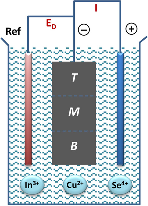
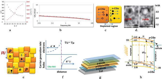
Pairing semiconductors with electrochemical processing offers an untapped opportunity to create novel nanostructures for practical devices. Here we report the results of one such pairing: the in-situ formation of highly-doped, interface-matched, sharp nanocrystalline homojunctions (NHJs) with single step electrodeposition of two copper-indium-selenide (CISe) compounds on flexible foil. It produces a homogenous film, comprising inherently ordered, 3-dimensional interconnected network of pn-CISe NHJs. These CISe NHJs exhibit surprising non-linear emissions, quantized transitions, large carrier mobility, low trap-state-density, long carrier lifetime and possible up-conversion. They facilitate efficient separation of minority carriers, reduce recombination and essentially function like quantum materials. This approach mitigates the material issues and complex fabrication of incumbent nanoscale heterojunctions; it also overcomes the flexibility and scale-up challenges of conventional planar pn junctions. The self-stabilized CISe NHJ film can be roll-to-roll processed in ambient atmosphere, thus providing a promising platform for a range of optoelectronic technologies. This concept exemplified by CISe compounds can be adapted to create nano-scale pn junctions with other inorganic semiconductors.
将半导体与电化学处理相结合,为制造用于实际设备的新型纳米结构提供了一个尚未开发的机会。在此,我们报告这样一种结合的结果:通过在柔性箔片上一步电沉积两种铜铟硒(CISe)化合物,原位形成高度掺杂、界面匹配的尖锐纳米晶同质结(NHJ)。它产生了一种均匀的薄膜,由pn-CISe NHJ的固有有序三维互连网络组成。这些CISe NHJ表现出令人惊讶的非线性发射、量子化跃迁、大载流子迁移率、低陷阱态密度、长载流子寿命以及可能的上转换。它们有助于少数载流子的有效分离,减少复合,本质上起到量子材料的作用。这种方法缓解了现有纳米级异质结的材料问题和复杂制造过程;它还克服了传统平面pn结的柔韧性和放大挑战。自稳定的CISe NHJ薄膜可以在环境气氛中进行卷对卷加工,从而为一系列光电子技术提供了一个有前景的平台。以CISe化合物为例的这一概念可适用于与其他无机半导体创建纳米级pn结。