Wen Qiuling, Wei Xinyu, Zhang Pengcheng, Lu Jing, Jiang Feng, Lu Xizhao
Institute of Manufacturing Engineering, Huaqiao University, Xiamen 361021, China.
MOE Engineering Research Center for Brittle Materials Machining, Institute of Manufacturing Engineering, Huaqiao University, Xiamen 361021, China.
Micromachines (Basel). 2021 May 26;12(6):611. doi: 10.3390/mi12060611.
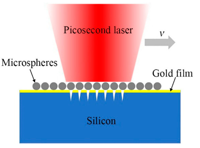
The nanohole arrays on the silicon substrate can effectively enhance the light absorption in thin film silicon solar cells. In order to optimize the solar energy absorption, polystyrene microspheres with diameters of 1 μm are used to assist picosecond laser with a wavelength of 1064 nm to fabricate nanohole arrays on silicon substrate. The experimental results show that the morphology and size of the silicon nanoholes strongly depend on the laser fluence. At 1.19-1.59 J/cm laser fluences, well-ordered arrays of nanoholes were fabricated on silicon substrate, with diameters domain from 250 to 549 nm and depths ranging from 60 to 99 nm. However, large amounts of sputtered nanoparticles appeared around the silicon nanoholes. To improve the surface morphology of silicon nanoholes, a nanolayered gold coating is applied on silicon surface to assist laser processing. The results show that, for gold-coated silicon substrate, sputtered nanoparticles around the nanoholes are almost invisible and the cross-sectional profiles of the nanoholes are smoother. Moreover, the ablation rate of the nanoholes on the gold-coated silicon substrate have increased compared to that of the nanoholes on the uncoated one. This simple method allows fast fabrication of well-ordered nanoholes on silicon substrate without sputtered nanoparticles and with smooth inner surface.
硅衬底上的纳米孔阵列能够有效增强薄膜硅太阳能电池中的光吸收。为了优化太阳能吸收,使用直径为1μm的聚苯乙烯微球辅助波长为1064nm的皮秒激光在硅衬底上制备纳米孔阵列。实验结果表明,硅纳米孔的形貌和尺寸强烈依赖于激光能量密度。在1.19 - 1.59J/cm的激光能量密度下,在硅衬底上制备出了排列有序的纳米孔阵列,其直径范围为250至549nm,深度范围为60至99nm。然而,在硅纳米孔周围出现了大量溅射的纳米颗粒。为了改善硅纳米孔的表面形貌,在硅表面施加一层纳米金涂层以辅助激光加工。结果表明,对于涂有金的硅衬底,纳米孔周围溅射的纳米颗粒几乎不可见,并且纳米孔的横截面轮廓更平滑。此外,与未涂覆的硅衬底上的纳米孔相比,涂有金的硅衬底上纳米孔的烧蚀速率有所提高。这种简单方法能够在硅衬底上快速制备出排列有序、无溅射纳米颗粒且内表面光滑的纳米孔。