Houtsma R S Koen, de la Rie Joris, Stöhr Meike
Zernike Institute for Advanced Materials, University of Groningen, Nijenborgh 4, 9747AG, Groningen, The Netherlands.
Chem Soc Rev. 2021 Jun 8;50(11):6541-6568. doi: 10.1039/d0cs01541e.
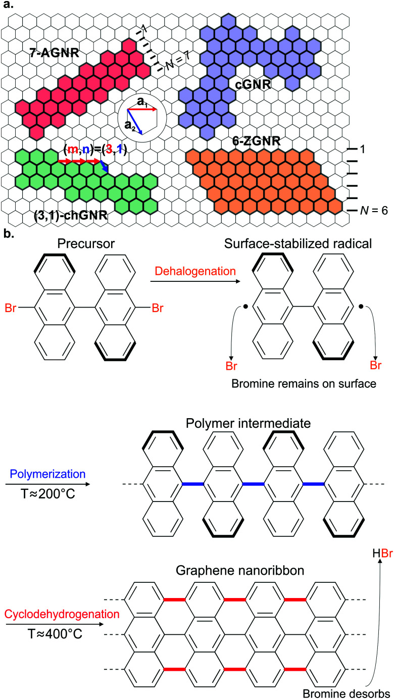
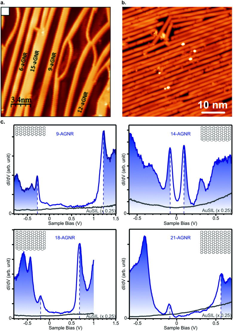
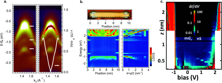
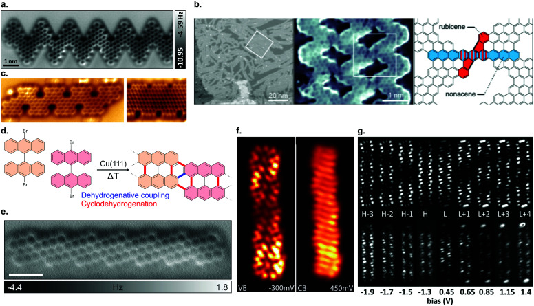
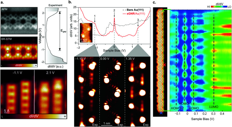
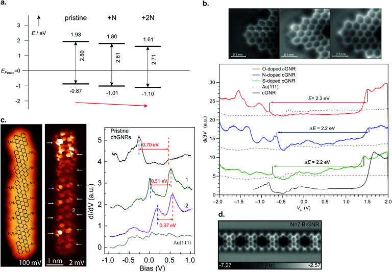
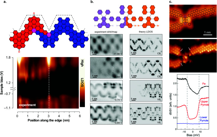
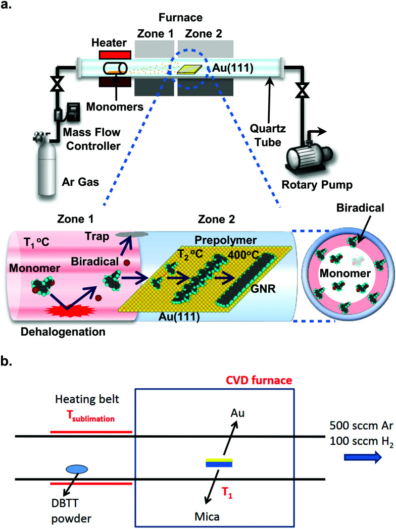
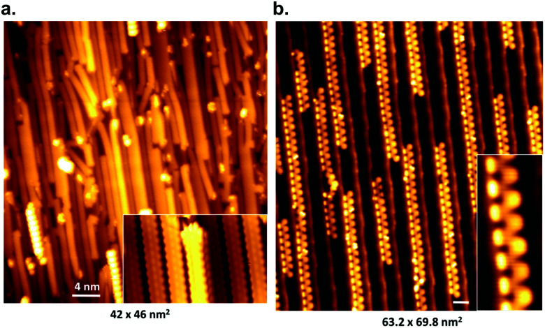
Graphene nanoribbons hold great promise for future applications in nanoelectronic devices, as they may combine the excellent electronic properties of graphene with the opening of an electronic band gap - not present in graphene but required for transistor applications. With a two-step on-surface synthesis process, graphene nanoribbons can be fabricated with atomic precision, allowing precise control over width and edge structure. Meanwhile, a decade of research has resulted in a plethora of graphene nanoribbons having various structural and electronic properties. This article reviews not only the on-surface synthesis of atomically precise graphene nanoribbons but also how their electronic properties are ultimately linked to their structure. Current knowledge and considerations with respect to precursor design, which eventually determines the final (electronic) structure, are summarized. Special attention is dedicated to the electronic properties of graphene nanoribbons, also in dependence on their width and edge structure. It is exactly this possibility of precisely changing their properties by fine-tuning the precursor design - offering tunability over a wide range - which has generated this vast research interest, also in view of future applications. Thus, selected device prototypes are presented as well.
石墨烯纳米带在未来纳米电子器件应用中具有巨大潜力,因为它们可能将石墨烯的优异电子特性与电子带隙的打开相结合——石墨烯中不存在带隙,但晶体管应用需要带隙。通过两步表面合成工艺,可以以原子精度制造石墨烯纳米带,从而实现对宽度和边缘结构的精确控制。同时,经过十年的研究,已经产生了大量具有各种结构和电子特性的石墨烯纳米带。本文不仅综述了原子精确的石墨烯纳米带的表面合成,还阐述了它们的电子特性最终如何与其结构相关联。总结了关于前体设计的当前知识和考虑因素,前体设计最终决定了最终的(电子)结构。特别关注了石墨烯纳米带的电子特性,这些特性也取决于它们的宽度和边缘结构。正是通过微调前体设计精确改变其特性的这种可能性——在很宽的范围内提供可调性——引发了如此广泛的研究兴趣,也考虑到了未来的应用。因此,还展示了选定的器件原型。