Pennelli Giovanni, Dimaggio Elisabetta, Masci Antonella
Dipartimento di Ingegneria dell'Informazione, Università di Pisa, Via G.Caruso, I-56122 Pisa, Italy.
Materials (Basel). 2021 Sep 14;14(18):5305. doi: 10.3390/ma14185305.
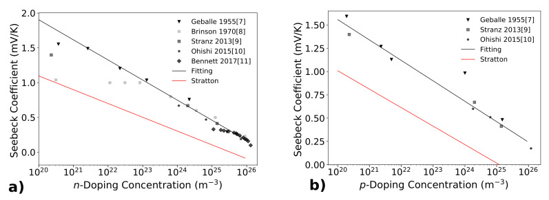
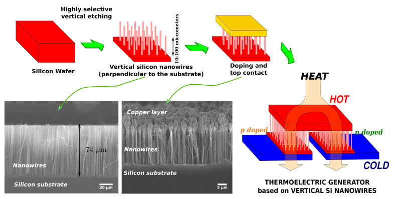
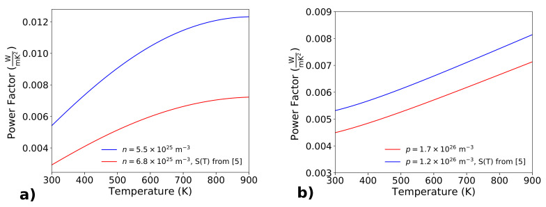
The potentialities of silicon as a starting material for electronic devices are well known and largely exploited, driving the worldwide spreading of integrated circuits. When nanostructured, silicon is also an excellent material for thermoelectric applications, and hence it could give a significant contribution in the fundamental fields of energy micro-harvesting (scavenging) and macro-harvesting. On the basis of recently published experimental works, we show that the power factor of silicon is very high in a large temperature range (from room temperature up to 900 K). Combining the high power factor with the reduced thermal conductivity of monocrystalline silicon nanowires and nanostructures, we show that the foreseen figure of merit ZT could be very high, reaching values well above 1 at temperatures around 900 K. We report the best parameters to optimize the thermoelectric properties of silicon nanostructures, in terms of doping concentration and nanowire diameter. At the end, we report some technological processes and solutions for the fabrication of macroscopic thermoelectric devices, based on large numbers of silicon nanowire/nanostructures, showing some fabricated demonstrators.
硅作为电子器件起始材料的潜力广为人知且得到了大量开发,推动了集成电路在全球的普及。当制成纳米结构时,硅也是热电应用的极佳材料,因此它能在能量微采集( scavenging )和宏采集这些基础领域做出重大贡献。基于最近发表的实验成果,我们表明硅的功率因数在很大温度范围(从室温到900 K )内都非常高。结合高功率因数与单晶硅纳米线和纳米结构降低的热导率,我们表明预计的优值ZT可能非常高,在900 K左右的温度下能达到远高于1的值。我们报告了在掺杂浓度和纳米线直径方面优化硅纳米结构热电性能的最佳参数。最后,我们报告了基于大量硅纳米线/纳米结构制造宏观热电器件的一些工艺流程和解决方案,并展示了一些已制造出的演示器件。