Arjmand Tabassom, Legallais Maxime, Nguyen Thi Thu Thuy, Serre Pauline, Vallejo-Perez Monica, Morisot Fanny, Salem Bassem, Ternon Céline
Univ. Grenoble Alpes, CNRS, Grenoble INP (Institute of Engineering Univ. Grenoble Alpes), LMGP, F-38000 Grenoble, France.
Univ. Grenoble Alpes, CNRS, Grenoble INP (Institute of Engineering Univ. Grenoble Alpes), IMEP-LAHC, F-38000 Grenoble, France.
Nanomaterials (Basel). 2022 Mar 22;12(7):1043. doi: 10.3390/nano12071043.
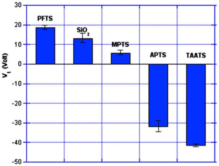
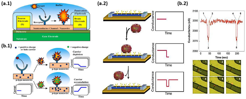
This paper summarizes some of the essential aspects for the fabrication of functional devices from bottom-up silicon nanowires. In a first part, the different ways of exploiting nanowires in functional devices, from single nanowires to large assemblies of nanowires such as nanonets (two-dimensional arrays of randomly oriented nanowires), are briefly reviewed. Subsequently, the main properties of nanowires are discussed followed by those of nanonets that benefit from the large numbers of nanowires involved. After describing the main techniques used for the growth of nanowires, in the context of functional device fabrication, the different techniques used for nanowire manipulation are largely presented as they constitute one of the first fundamental steps that allows the nanowire positioning necessary to start the integration process. The advantages and disadvantages of each of these manipulation techniques are discussed. Then, the main families of nanowire-based transistors are presented; their most common integration routes and the electrical performance of the resulting devices are also presented and compared in order to highlight the relevance of these different geometries. Because they can be bottlenecks, the key technological elements necessary for the integration of silicon nanowires are detailed: the sintering technique, the importance of surface and interface engineering, and the key role of silicidation for good device performance. Finally the main application areas for these silicon nanowire devices are reviewed.
本文总结了自下而上制备硅纳米线功能器件的一些关键方面。在第一部分,简要回顾了在功能器件中利用纳米线的不同方式,从单根纳米线到纳米线的大型组件,如纳米网(随机取向纳米线的二维阵列)。随后,讨论了纳米线的主要特性,接着是受益于大量纳米线的纳米网的特性。在描述了用于纳米线生长的主要技术之后,在功能器件制造的背景下,大量介绍了用于纳米线操纵的不同技术,因为它们构成了启动集成过程所需的纳米线定位的首要基本步骤之一。讨论了每种操纵技术的优缺点。然后,介绍了基于纳米线的晶体管的主要类别;还介绍并比较了它们最常见的集成路线以及所得器件的电学性能,以突出这些不同几何结构的相关性。由于它们可能成为瓶颈,详细介绍了硅纳米线集成所需的关键技术要素:烧结技术、表面和界面工程的重要性以及硅化对良好器件性能的关键作用。最后回顾了这些硅纳米线器件的主要应用领域。