Wang Yang, Cheng Yu, Wang Yunlu, Zhang Shuai, Zhang Xuewei, Yin Shaoqian, Wang Miao, Xia Yang, Li Qunyang, Zhao Pei, Wang Hongtao
Institute of Applied Mechanics, Key Laboratory of Soft Machines and Smart Devices of Zhejiang Province, Zhejiang University Hangzhou 310012 P. R. China
Center for Nano and Micro Mechanics, Applied Mechanics Laboratory, School of Aerospace Engineering, Tsinghua University Beijing 100084 P. R. China.
RSC Adv. 2018 Feb 26;8(16):8800-8804. doi: 10.1039/c8ra00770e. eCollection 2018 Feb 23.
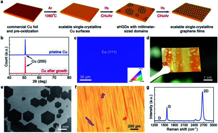
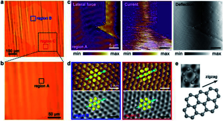
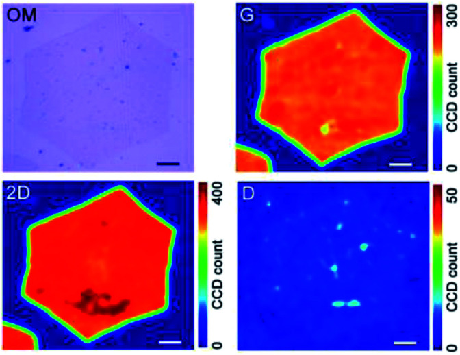
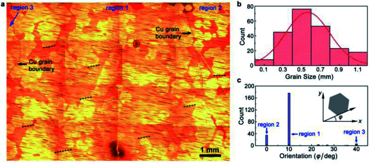
Chemical vapor deposition (CVD) is considered as an effective route to obtain large-area and high-quality polycrystalline graphene; however, there are still technological challenges associated with its application to achieve single crystals of graphene. Herein, we present the CVD growth of scalable single-crystalline graphene by seamless stitching millimeter-sized unidirectional aligned hexagonal domains using different types of commercial Cu foils without repeated substrate polishing and H-annealing processes. Compared with that reported in previous studies, herein, the average size for the hexagonal graphene domains is enlarged by 1-2 orders of magnitude (from tens of micrometers to millimeter). The key factor for growth is the Cu surface monocrystallization achieved by a pre-introduced oxide layer and the sequential Ar annealing. The graphene domains exhibit an average growth rate of >20 μm min and a misorientation possibility of <2%, and seamless stitching at the domain coalescence interfaces is confirmed by atomic force microscopy measurements.
化学气相沉积(CVD)被认为是获得大面积高质量多晶石墨烯的有效途径;然而,将其应用于实现石墨烯单晶仍存在技术挑战。在此,我们展示了通过使用不同类型的商用铜箔无缝拼接毫米级单向排列的六边形畴来实现可扩展单晶石墨烯的CVD生长,无需重复的衬底抛光和H退火工艺。与先前研究报道的相比,此处六边形石墨烯畴的平均尺寸扩大了1 - 2个数量级(从几十微米到毫米)。生长的关键因素是通过预先引入的氧化层和随后的氩气退火实现的铜表面单晶化。石墨烯畴的平均生长速率>20μm/min,取向差可能性<2%,并且通过原子力显微镜测量证实了畴合并界面处的无缝拼接。