Ranjan Pranay, Gaur Snehraj, Yadav Himanshu, Urgunde Ajay B, Singh Vikas, Patel Avit, Vishwakarma Kusum, Kalirawana Deepak, Gupta Ritu, Kumar Prashant
Department of Metallurgical and Materials Engineering, Indian Institute of Technology Jodhpur, Karwar, 342037, Rajasthan, India.
Advanced Materials and Devices Laboratory, Department of Chemistry, Indian Institute of Technology Jodhpur, Karwar, 342037, Rajasthan, India.
Nano Converg. 2022 Jun 6;9(1):26. doi: 10.1186/s40580-022-00317-7.
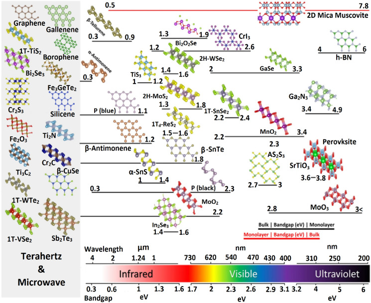
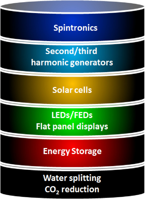
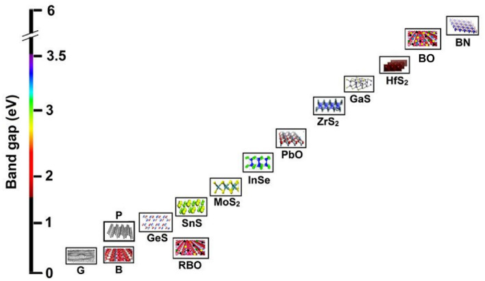
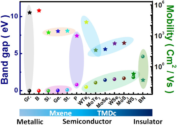
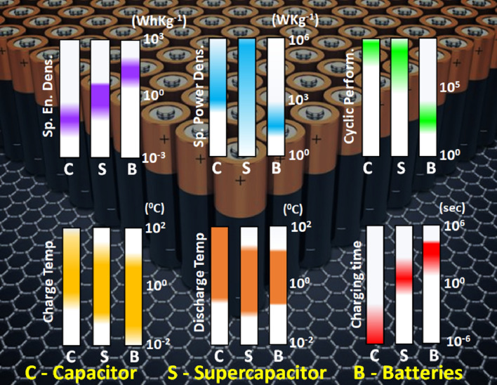
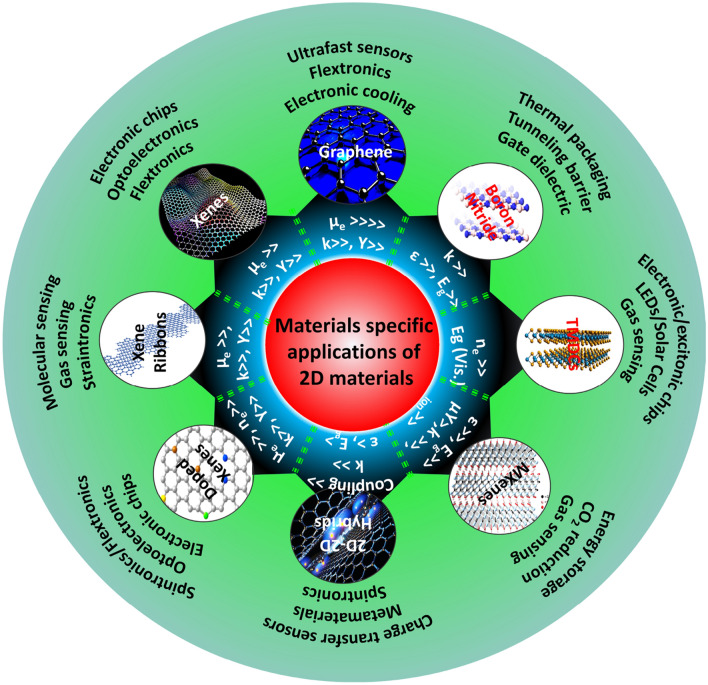
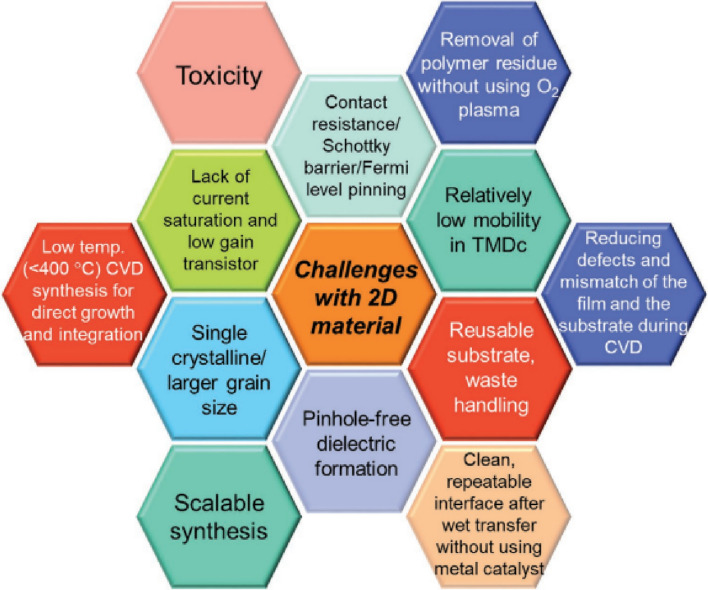
Quantum flatland i.e., the family of two dimensional (2D) quantum materials has become increscent and has already encompassed elemental atomic sheets (Xenes), 2D transition metal dichalcogenides (TMDCs), 2D metal nitrides/carbides/carbonitrides (MXenes), 2D metal oxides, 2D metal phosphides, 2D metal halides, 2D mixed oxides, etc. and still new members are being explored. Owing to the occurrence of various structural phases of each 2D material and each exhibiting a unique electronic structure; bestows distinct physical and chemical properties. In the early years, world record electronic mobility and fractional quantum Hall effect of graphene attracted attention. Thanks to excellent electronic mobility, and extreme sensitivity of their electronic structures towards the adjacent environment, 2D materials have been employed as various ultrafast precision sensors such as gas/fire/light/strain sensors and in trace-level molecular detectors and disease diagnosis. 2D materials, their doped versions, and their hetero layers and hybrids have been successfully employed in electronic/photonic/optoelectronic/spintronic and straintronic chips. In recent times, quantum behavior such as the existence of a superconducting phase in moiré hetero layers, the feasibility of hyperbolic photonic metamaterials, mechanical metamaterials with negative Poisson ratio, and potential usage in second/third harmonic generation and electromagnetic shields, etc. have raised the expectations further. High surface area, excellent young's moduli, and anchoring/coupling capability bolster hopes for their usage as nanofillers in polymers, glass, and soft metals. Even though lab-scale demonstrations have been showcased, large-scale applications such as solar cells, LEDs, flat panel displays, hybrid energy storage, catalysis (including water splitting and CO reduction), etc. will catch up. While new members of the flatland family will be invented, new methods of large-scale synthesis of defect-free crystals will be explored and novel applications will emerge, it is expected. Achieving a high level of in-plane doping in 2D materials without adding defects is a challenge to work on. Development of understanding of inter-layer coupling and its effects on electron injection/excited state electron transfer at the 2D-2D interfaces will lead to future generation heterolayer devices and sensors.
量子二维领域,即二维量子材料家族,正日益壮大,已经涵盖了元素原子薄片(烯类)、二维过渡金属硫族化合物(TMDCs)、二维金属氮化物/碳化物/碳氮化物(MXenes)、二维金属氧化物、二维金属磷化物、二维金属卤化物、二维混合氧化物等,并且仍在探索新的成员。由于每种二维材料都存在各种结构相,且每种相都具有独特的电子结构,赋予了其独特的物理和化学性质。早年,石墨烯创世界纪录的电子迁移率和分数量子霍尔效应引起了关注。由于具有出色的电子迁移率,以及其电子结构对相邻环境的极端敏感性,二维材料已被用作各种超快精密传感器,如气体/火灾/光/应变传感器、痕量分子探测器和疾病诊断。二维材料、其掺杂版本、其异质层和杂化物已成功应用于电子/光子/光电子/自旋电子和应变电子芯片。近年来,诸如莫尔异质层中超导相的存在、双曲光子超材料的可行性、具有负泊松比的机械超材料以及在二次/三次谐波产生和电磁屏蔽等方面的潜在应用等量子行为,进一步提高了人们的期望。高表面积、出色的杨氏模量以及锚固/耦合能力,增强了它们作为聚合物、玻璃和软金属中纳米填料使用的希望。尽管已经展示了实验室规模的演示,但太阳能电池、发光二极管、平板显示器、混合储能、催化(包括水分解和一氧化碳还原)等大规模应用将会跟进。预计在发明二维领域家族新成员的同时,将探索无缺陷晶体的大规模合成新方法,并出现新的应用。在二维材料中不引入缺陷地实现高水平的面内掺杂是一项有待攻克的挑战。对层间耦合及其对二维 - 二维界面处电子注入/激发态电子转移影响的理解发展,将引领下一代异质层器件和传感器的发展。