Wang Yunhao, Wu Sheng, Wang Wenjing, Wu Tao, Li Xinxin
State Key Laboratory of Transducer Technology, Shanghai Institute of Microsystem and Information Technology, Chinese Academy of Sciences, Shanghai 200050, China.
School of Information Science and Technology, ShanghaiTech University, Shanghai 201210, China.
Micromachines (Basel). 2024 Mar 30;15(4):482. doi: 10.3390/mi15040482.
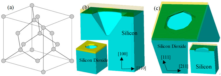
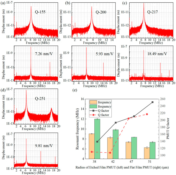
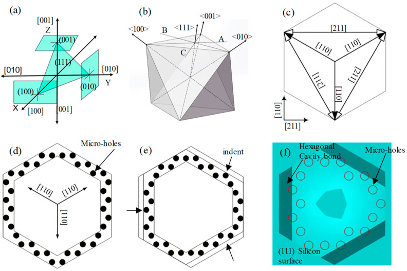
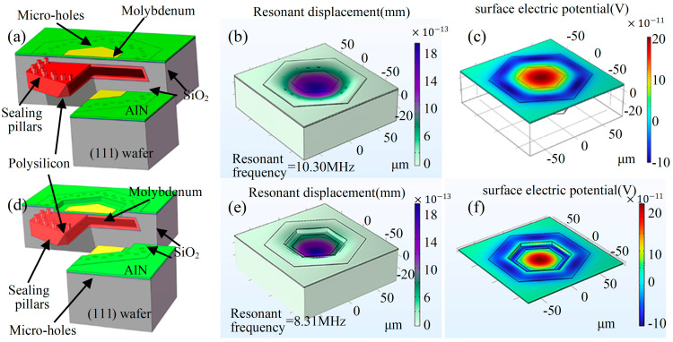
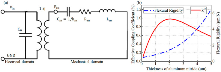
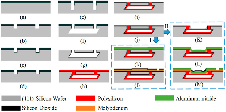
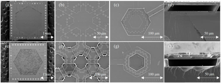
Piezoelectric micromachined ultrasound transducers (PMUTs) have gained significant popularity in the field of ultrasound ranging and medical imaging owing to their small size, low power consumption, and affordability. The scar-free "MIS" (micro-hole inter-etch and sealing) process, a novel bulk-silicon manufacturing technique, has been successfully developed for the fabrication of pressure sensors, flow sensors, and accelerometers. In this study, we utilize the MIS process to fabricate cavity diaphragm structures for PMUTs, resulting in the formation of a flat cavity diaphragm structure through anisotropic etching of (111) wafers in a 70 °C tetramethylammonium hydroxide (TMAH) solution. This study investigates the corrosion characteristics of the MIS technology on (111) silicon wafers, arranges micro-pores etched on bulk silicon around the desired cavity structure in a regular pattern, and takes into consideration the distance compensation for lateral corrosion, resulting in a fully connected cavity structure closely approximating an ortho-hexagonal shape. By utilizing a sputtering process to deposit metallic molybdenum as upper and lower electrodes, as well as piezoelectric materials above the cavity structure, we have successfully fabricated aluminum nitride (AlN) piezoelectric ultrasonic transducer arrays of various sizes and structures. The final hexagonal PMUT cells of various sizes that were fabricated achieved a maximum quality factor (Q) of 251 and a displacement sensitivity of 18.49 nm/V across a range of resonant frequencies from 6.28 MHz to 11.99 MHz. This fabrication design facilitates the achievement of IC-compatible and cost-effective mass production of PMUT array devices with high resonance frequencies.
压电微机械超声换能器(PMUT)由于其尺寸小、功耗低且价格实惠,在超声测距和医学成像领域已获得显著的普及。无疤痕的“MIS”(微孔互蚀刻和密封)工艺,一种新型的体硅制造技术,已成功开发用于制造压力传感器、流量传感器和加速度计。在本研究中,我们利用MIS工艺制造用于PMUT的腔膜结构,通过在70°C的四甲基氢氧化铵(TMAH)溶液中对(111)晶圆进行各向异性蚀刻,形成扁平的腔膜结构。本研究调查了MIS技术在(111)硅晶圆上的腐蚀特性,将在体硅上蚀刻的微孔以规则图案排列在所需的腔结构周围,并考虑横向腐蚀的距离补偿,从而得到一个紧密近似正六边形形状的完全连通的腔结构。通过利用溅射工艺沉积金属钼作为上下电极以及在腔结构上方沉积压电材料,我们成功制造了各种尺寸和结构的氮化铝(AlN)压电超声换能器阵列。所制造的各种尺寸的最终六边形PMUT单元在6.28 MHz至11.99 MHz的一系列共振频率范围内实现了最大品质因数(Q)为251和位移灵敏度为18.49 nm/V。这种制造设计有助于实现具有高共振频率的PMUT阵列器件的IC兼容且经济高效的大规模生产。