Liu Zhibo, Wang Lei, Hong Yi-Lun, Chen Xing-Qiu, Cheng Hui-Ming, Ren Wencai
Shenyang National Laboratory for Materials Science, Institute of Metal Research, Chinese Academy of Sciences, Shenyang 110016, China.
School of Materials Science and Engineering, University of Science and Technology of China, Shenyang 110016, China.
Natl Sci Rev. 2022 Nov 28;10(4):nwac273. doi: 10.1093/nsr/nwac273. eCollection 2023 Apr.
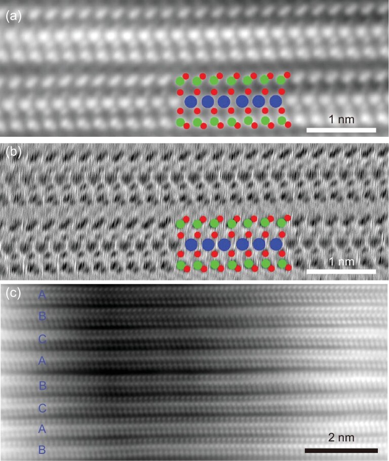
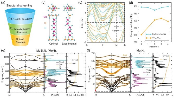
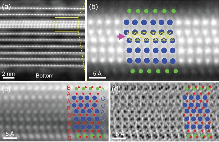
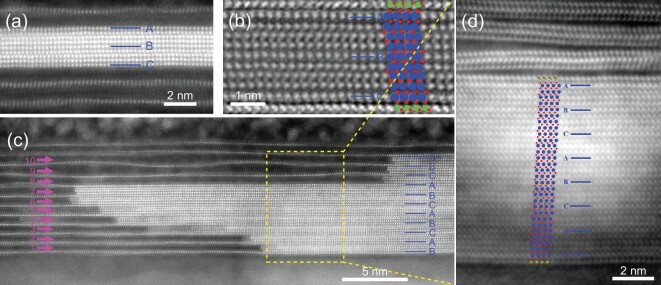
The number and stacking order of layers are two important degrees of freedom that can modulate the properties of 2D van der Waals (vdW) materials. However, the layers' structures are essentially limited to the known layered 3D vdW materials. Recently, a new 2D vdW material, MoSiN, without known 3D counterparts, was synthesized by passivating the surface dangling bonds of non-layered 2D molybdenum nitride with elemental silicon, whose monolayer can be viewed as a monolayer MoN (-N-Mo-N-) sandwiched between two Si-N layers. This unique sandwich structure endows the MoSiN monolayer with many fascinating properties and intriguing applications, and the surface-passivating growth method creates the possibility of tuning the layer's structure of 2D vdW materials. Here we synthesized a series of MoSiN(MoN) structures confined in the matrix of multilayer MoSiN. These super-thick monolayers are the homologous compounds of MoSiN, which can be viewed as multilayer MoN (MoN) sandwiched between two Si-N layers. First-principles calculations show that MoSiN(MoN) monolayers have much higher Young's modulus than MoN, which is attributed to the strong Si-N bonds on the surface. Importantly, different from the semiconducting nature of the MoSiN monolayer, the MoSiN(MoN) monolayer is identified as a superconductor with a transition temperature of 9.02 K. The discovery of MoSiN(MoN) structures not only expands the family of 2D materials but also brings a new degree of freedom to tailor the structure of 2D vdW materials, which may lead to unexpected novel properties and applications.
层的数量和堆叠顺序是两个重要的自由度,可调节二维范德华(vdW)材料的性质。然而,层结构本质上局限于已知的层状三维vdW材料。最近,一种没有已知三维对应物的新型二维vdW材料MoSiN通过用元素硅钝化非层状二维氮化钼的表面悬空键而合成,其单层可视为夹在两个Si-N层之间的单层MoN(-N-Mo-N-)。这种独特的夹心结构赋予MoSiN单层许多迷人的特性和有趣的应用,并且表面钝化生长方法为调节二维vdW材料的层结构创造了可能性。在这里,我们合成了一系列限制在多层MoSiN基质中的MoSiN(MoN)结构。这些超厚单层是MoSiN的同系化合物,可视为夹在两个Si-N层之间的多层MoN(MoN)。第一性原理计算表明,MoSiN(MoN)单层的杨氏模量比MoN高得多,这归因于表面上强的Si-N键。重要的是,与MoSiN单层的半导体性质不同,MoSiN(MoN)单层被确定为一种转变温度为9.02 K的超导体。MoSiN(MoN)结构的发现不仅扩展了二维材料家族,还为定制二维vdW材料的结构带来了新的自由度,这可能导致意想不到的新颖特性和应用。