Van Damme J, Massar S, Acharya R, Ivanov Ts, Perez Lozano D, Canvel Y, Demarets M, Vangoidsenhoven D, Hermans Y, Lai J G, Vadiraj A M, Mongillo M, Wan D, De Boeck J, Potočnik A, De Greve K
Imec, Leuven, Belgium.
Department of Electrical Engineering (ESAT), KU Leuven, Leuven, Belgium.
Nature. 2024 Oct;634(8032):74-79. doi: 10.1038/s41586-024-07941-9. Epub 2024 Sep 18.
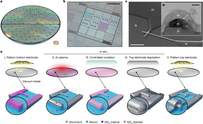
The development of superconducting qubit technology has shown great potential for the construction of practical quantum computers. As the complexity of quantum processors continues to grow, the need for stringent fabrication tolerances becomes increasingly critical. Utilizing advanced industrial fabrication processes could facilitate the necessary level of fabrication control to support the continued scaling of quantum processors. However, at present, these industrial processes are not optimized to produce high-coherence devices, nor are they a priori compatible with the approaches commonly used to make superconducting qubits. Here we demonstrate superconducting transmon qubits manufactured in a 300 mm complementary metal-oxide-semiconductor (CMOS) pilot line using industrial fabrication methods, with resulting relaxation and coherence times exceeding 100 μs. We show across-wafer, large-scale statistics of coherence, yield, variability and ageing that confirm the validity of our approach. The presented industry-scale fabrication process, which uses only optical lithography and reactive-ion etching, has a performance and yield in line with conventional laboratory-style techniques utilizing metal lift-off, angled evaporation and electron-beam writing. Moreover, it offers the potential for further upscaling through three-dimensional integration and more process optimization. This result marks the advent of an alternative and new, large-scale, truly CMOS-compatible fabrication method for superconducting quantum computing processors.
超导量子比特技术的发展已显示出构建实用量子计算机的巨大潜力。随着量子处理器的复杂性不断增加,对严格制造公差的需求变得越来越关键。利用先进的工业制造工艺可以促进必要的制造控制水平,以支持量子处理器的持续扩展。然而,目前这些工业工艺并未针对生产高相干性器件进行优化,也并非先验地与制造超导量子比特常用的方法兼容。在此,我们展示了使用工业制造方法在300毫米互补金属氧化物半导体(CMOS)中试生产线上制造的超导transmon量子比特,其弛豫时间和相干时间超过100微秒。我们展示了全晶圆、大规模的相干性、良率、可变性和老化统计数据,证实了我们方法的有效性。所展示的工业规模制造工艺仅使用光刻和反应离子蚀刻,其性能和良率与采用金属剥离、倾斜蒸发和电子束光刻的传统实验室式技术相当。此外,它还具有通过三维集成和更多工艺优化进一步扩大规模的潜力。这一成果标志着一种用于超导量子计算处理器的全新、大规模、真正与CMOS兼容的制造方法的出现。