Guo Xinghan, Xie Mouzhe, Addhya Anchita, Linder Avery, Zvi Uri, Wang Stella, Yu Xiaofei, Deshmukh Tanvi D, Liu Yuzi, Hammock Ian N, Li Zixi, DeVault Clayton T, Butcher Amy, Esser-Kahn Aaron P, Awschalom David D, Delegan Nazar, Maurer Peter C, Heremans F Joseph, High Alexander A
Pritzker School of Molecular Engineering, University of Chicago, Chicago, IL, 60637, USA.
School of Molecular Sciences, Arizona State University, Tempe, AZ, 85287, USA.
Nat Commun. 2024 Oct 10;15(1):8788. doi: 10.1038/s41467-024-53150-3.
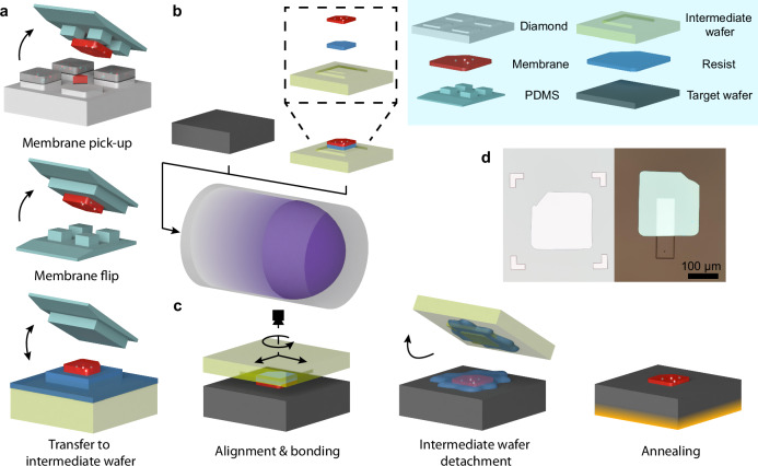
Diamond has superlative material properties for a broad range of quantum and electronic technologies. However, heteroepitaxial growth of single crystal diamond remains limited, impeding integration and evolution of diamond-based technologies. Here, we directly bond single-crystal diamond membranes to a wide variety of materials including silicon, fused silica, sapphire, thermal oxide, and lithium niobate. Our bonding process combines customized membrane synthesis, transfer, and dry surface functionalization, allowing for minimal contamination while providing pathways for near unity yield and scalability. We generate bonded crystalline membranes with thickness as low as 10 nm, sub-nm interfacial regions, and nanometer-scale thickness variability over 200 by 200 μm areas. We measure spin coherence times T for nitrogen vacancy centers in 150 nm-thick bonded membranes of up to 623 ± 21 μs, suitable for advanced quantum applications. We demonstrate multiple methods for integrating high quality factor nanophotonic cavities with the diamond heterostructures, highlighting the platform versatility in quantum photonic applications. Furthermore, we show that our ultra-thin diamond membranes are compatible with total internal reflection fluorescence (TIRF) microscopy, which enables interfacing coherent diamond quantum sensors with living cells while rejecting unwanted background luminescence. The processes demonstrated herein provide a full toolkit to synthesize heterogeneous diamond-based hybrid systems for quantum and electronic technologies.
对于广泛的量子和电子技术而言,金刚石具有卓越的材料特性。然而,单晶金刚石的异质外延生长仍然受限,这阻碍了基于金刚石的技术的集成与发展。在此,我们将单晶金刚石膜直接键合到多种材料上,包括硅、熔融石英、蓝宝石、热氧化物和铌酸锂。我们的键合工艺结合了定制的膜合成、转移和干式表面功能化,在实现近乎统一的产率和可扩展性的同时,将污染降至最低。我们制备出了厚度低至10纳米、界面区域小于1纳米且在200×200微米区域内具有纳米级厚度变化的键合晶体膜。我们测量了150纳米厚的键合膜中氮空位中心的自旋相干时间T,长达623±21微秒,适用于先进的量子应用。我们展示了多种将高品质因子纳米光子腔与金刚石异质结构集成的方法,凸显了该平台在量子光子应用中的多功能性。此外,我们表明我们的超薄金刚石膜与全内反射荧光(TIRF)显微镜兼容,这使得相干金刚石量子传感器能够与活细胞连接,同时抑制不需要的背景发光。本文展示的工艺提供了一整套工具,用于合成用于量子和电子技术的基于金刚石的异质混合系统。