Kim DoYoung, Ryu Seong, Bae Sukang, Lee Min Wook, Kim Tae-Wook, Bae Jong-Seong, Park Jiwon, Lee Seoung-Ki
School of Material Science and Engineering, Pusan National University, Busan 46241, Republic of Korea.
Institute of Advanced Composite Materials, Korea Institute of Science and Technology (KIST), 92 Chudong-ro, Bongdong-eup, Wanju 55324, Republic of Korea.
Nanomaterials (Basel). 2024 Nov 29;14(23):1926. doi: 10.3390/nano14231926.
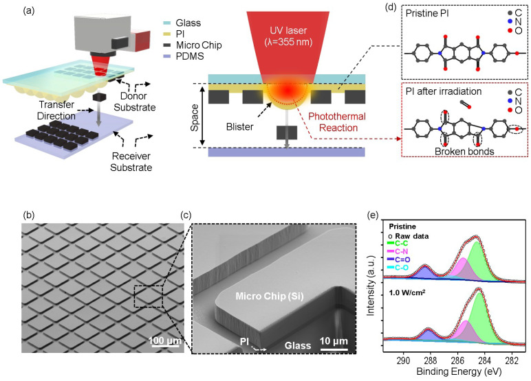
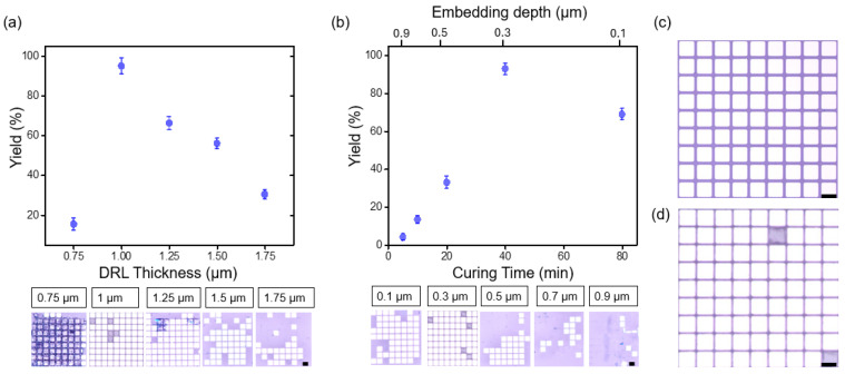
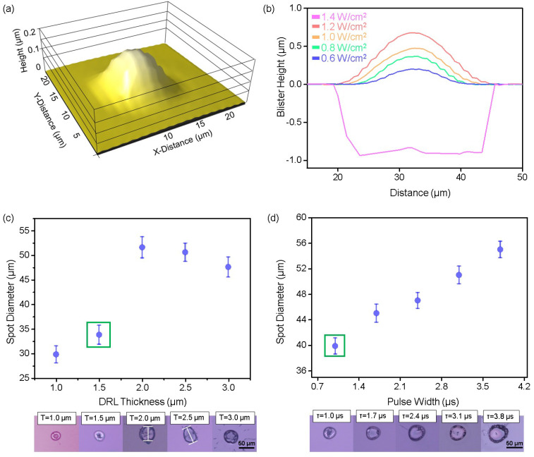
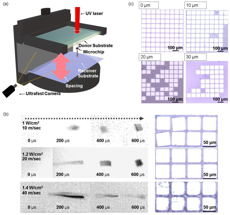
The rapid evolution of microelectronics and display technologies has driven the demand for advanced manufacturing techniques capable of precise, high-speed microchip transfer. As devices shrink in size and increase in complexity, scalable and contactless methods for microscale placement are essential. Laser-induced forward transfer (LIFT) has emerged as a transformative solution, offering the precision and adaptability required for next-generation applications such as micro-light-emitting diodes (μ-LEDs). This study optimizes the LIFT process for the precise transfer of silicon microchips designed to mimic μ-LEDs. Critical parameters, including laser energy density, laser pulse width, and dynamic release layer (DRL) thickness are systematically adjusted to ensure controlled blister formation, a key factor for successful material transfer. The DRL, a polyimide-based photoreactive layer, undergoes photothermal decomposition under 355 nm laser irradiation, creating localized pressure that propels microchips onto the receiver substrate in a contactless manner. Using advanced techniques such as three-dimensional profilometry, X-ray photoelectron spectroscopy, and ultrafast imaging, this study evaluates the rupture dynamics of the DRL and the velocity of microchips during transfer. Optimization of the DRL thickness to 1 µm and a transfer velocity of 20 m s⁻ achieves a transfer yield of up to 97%, showcasing LIFT's potential in μ-LED manufacturing and semiconductor production.
微电子和显示技术的快速发展推动了对能够进行精确、高速微芯片转移的先进制造技术的需求。随着器件尺寸缩小和复杂度增加,用于微尺度放置的可扩展且非接触式方法至关重要。激光诱导正向转移(LIFT)已成为一种变革性解决方案,为诸如微发光二极管(μ-LED)等下一代应用提供所需的精度和适应性。本研究优化了LIFT工艺,以精确转移设计用于模拟μ-LED的硅微芯片。系统地调整包括激光能量密度、激光脉冲宽度和动态释放层(DRL)厚度在内的关键参数,以确保形成可控的气泡,这是成功进行材料转移的关键因素。DRL是一种基于聚酰亚胺的光反应层,在355 nm激光照射下会发生光热分解,产生局部压力,以非接触方式将微芯片推送到接收基板上。本研究使用三维轮廓测量、X射线光电子能谱和超快成像等先进技术,评估了DRL的破裂动力学以及微芯片在转移过程中的速度。将DRL厚度优化至1 µm且转移速度为20 m s⁻时,转移产率高达97%,展示了LIFT在μ-LED制造和半导体生产中的潜力。