Patel Jessica, Sharme Razia Khan, Quijada Manuel A, Rana Mukti M
Division of Physics, Engineering, Mathematics and Computer Sciences and Optical Science Center for Applied Research, Delaware State University, Dover, DE 19901, USA.
NASA Goddard Space Flight Center, Greenbelt, MD 20771, USA.
Nanomaterials (Basel). 2024 Dec 14;14(24):2013. doi: 10.3390/nano14242013.
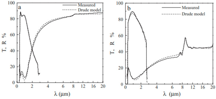
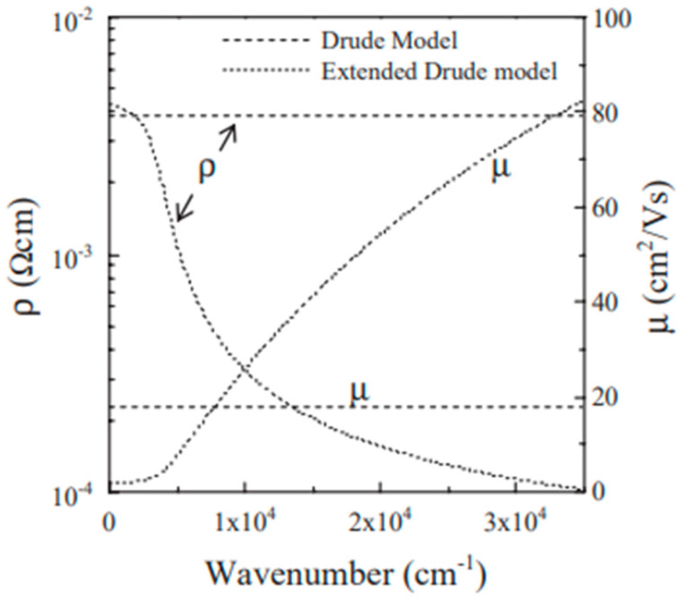
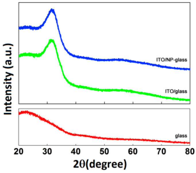
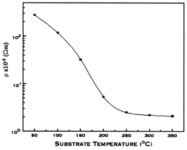
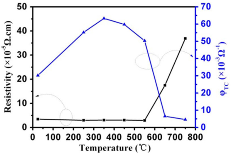
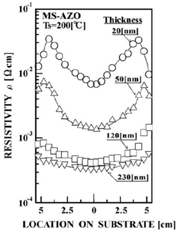
This study offers a comprehensive summary of the current states as well as potential future directions of transparent conducting oxides (TCOs), particularly tin-doped indium oxide (ITO), the most readily accessible TCO on the market. Solar cells, flat panel displays (FPDs), liquid crystal displays (LCDs), antireflection (AR) coatings for airbus windows, photovoltaic and optoelectronic devices, transparent p-n junction diodes, etc. are a few of the best uses for this material. Other conductive metals that show a lot of promise as substitutes for traditional conductive materials include copper, zinc oxide, aluminum, silver, gold, and tin. These metals are also utilized in AR coatings. The optimal deposition techniques for creating ITO films under the current conditions have been determined to be DC (direct current) and RF (radio frequency) MS (magnetron sputtering) deposition, both with and without the introduction of Ar gas. When producing most types of AR coatings, it is necessary to obtain thicknesses of at least 100 nm and minimum resistivities on the order of 10 Ω cm. For AR coatings, issues related to less-conductive materials than ITO have been considered.
本研究全面总结了透明导电氧化物(TCOs)的当前状况以及未来潜在发展方向,特别是市场上最易获取的TCO——氧化铟锡(ITO)。太阳能电池、平板显示器(FPDs)、液晶显示器(LCDs)、空客窗户的减反射(AR)涂层、光伏和光电器件、透明p-n结二极管等是这种材料的一些最佳应用。其他有望替代传统导电材料的导电金属包括铜、氧化锌、铝、银、金和锡。这些金属也用于AR涂层。在当前条件下制备ITO薄膜的最佳沉积技术已确定为直流(DC)和射频(RF)磁控溅射(MS)沉积,有无引入氩气均可。在生产大多数类型的AR涂层时,需要获得至少100nm的厚度以及约10Ω·cm的最小电阻率。对于AR涂层,已考虑了与比ITO导电性更低的材料相关的问题。