Lee Seung-Min, Jang Seong Cheol, Park Ji-Min, Park Jaewon, Choi Nayoung, Chung Kwun-Bum, Lee Jung Woo, Kim Hyun-Suk
Department of Materials Science and Engineering, Chungnam National University, Daejeon 34134, Republic of Korea.
Department of Energy and Materials Engineering, Dongguk University, Seoul 04620, Republic of Korea.
Nanomaterials (Basel). 2025 Mar 8;15(6):418. doi: 10.3390/nano15060418.
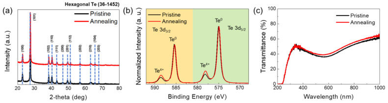
With the ongoing development of electronic devices, there is an increasing demand for new semiconductors beyond traditional silicon. A key element in electronic circuits, complementary metal-oxide semiconductor (CMOS), utilizes both n-type and p-type semiconductors. While the advancements in n-type semiconductors have been substantial, the development of high-mobility p-type semiconductors has lagged behind. Recently, tellurium (Te) has been recognized as a promising candidate due to its superior electrical properties and the capability for large-area deposition via vacuum processes. In this work, an innovative approach involving the addition of a metal-capping layer onto Te thin-film transistors (TFTs) is proposed, which significantly enhances their electrical characteristics. In particular, the application of an indium (In) metal-capping layer has led to a dramatic increase in the field-effect mobility of Te TFTs from 2.68 to 33.54 cm/Vs. This improvement is primarily due to the oxygen scavenger effect, which effectively minimizes oxidation and eliminates oxygen from the Te layer, resulting in the production of high-quality Te thin films. This progress in high-mobility p-type semiconductors is promising for the advancement of high-performance electronic devices in various applications and industries.
随着电子设备的不断发展,对传统硅以外的新型半导体的需求日益增加。电子电路中的关键元件互补金属氧化物半导体(CMOS)同时使用n型和p型半导体。虽然n型半导体取得了重大进展,但高迁移率p型半导体的发展却滞后了。最近,碲(Te)因其优异的电学性能以及通过真空工艺进行大面积沉积的能力而被认为是一种有前途的候选材料。在这项工作中,提出了一种在碲薄膜晶体管(TFT)上添加金属覆盖层的创新方法,该方法显著增强了它们的电学特性。特别是,铟(In)金属覆盖层的应用使碲TFT的场效应迁移率从2.68 cm²/V·s大幅提高到33.54 cm²/V·s。这种改进主要归因于除氧效应,它有效地减少了氧化并从碲层中去除了氧,从而生产出高质量的碲薄膜。高迁移率p型半导体的这一进展有望推动高性能电子设备在各种应用和行业中的发展。