Kim Jiwon, Hwang Inkook, Kim Byungwook, Lee Wookyung, Song Juha, Jung Yeonwoong, Yoon Changbun
Department of Advanced Materials Engineering, Tech University of Korea, Siheung-si 15073, Gyeonggi-do, Republic of Korea.
School of Chemistry, Chemical Engineering and Biotechnology, Nanyang Technological University, Singapore 637459, Singapore.
Nanomaterials (Basel). 2025 May 23;15(11):783. doi: 10.3390/nano15110783.
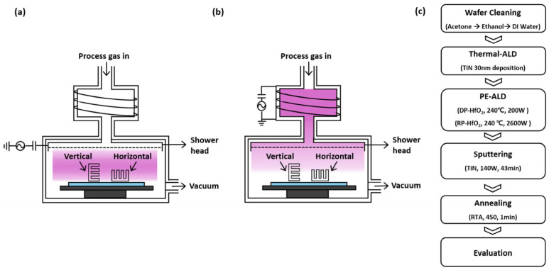
Dynamic random-access memory (DRAM) is a vital component in modern computing systems. Enhancing memory performance requires maximizing capacitor capacitance within DRAM cells, which is achieved using high-k dielectric materials deposited as thin, uniform films via atomic layer deposition (ALD). Precise film deposition that minimizes electronic defects caused by charged vacancies is essential for reducing leakage current and ensuring high dielectric strength. In this study, we fabricated metal-insulator-metal (MIM) capacitors in high-aspect-ratio trench structures using remote plasma ALD (RP-ALD) and direct plasma ALD (DP-ALD). The trenches, etched into silicon, featured a 7:1 aspect ratio, 76 nm pitch, and 38 nm critical dimension. We evaluated the electrical characteristics of HfO-based capacitors with TiN top and bottom electrodes, focusing on leakage current density and equivalent oxide thickness. Capacitance-voltage analysis and X-ray photoelectron spectroscopy (XPS) revealed that RP-ALD effectively suppressed plasma-induced damage, reducing defect density and leakage current. While DP-ALD offered excellent film properties, it suffered from degraded lateral uniformity due to direct plasma exposure. Given its superior lateral uniformity, lower leakage, and defect suppression, RP-ALD shows strong potential for improving DRAM capacitor performance and serves as a promising alternative to the currently adopted thermal ALD process.
动态随机存取存储器(DRAM)是现代计算系统中的一个重要组件。提高内存性能需要最大化DRAM单元内的电容器电容,这可以通过原子层沉积(ALD)以薄而均匀的薄膜形式沉积高k介电材料来实现。精确的薄膜沉积可将由带电空位引起的电子缺陷降至最低,这对于降低漏电流和确保高介电强度至关重要。在本研究中,我们使用远程等离子体ALD(RP-ALD)和直接等离子体ALD(DP-ALD)在高纵横比沟槽结构中制造了金属-绝缘体-金属(MIM)电容器。蚀刻到硅中的沟槽具有7:1的纵横比、76 nm的间距和38 nm的关键尺寸。我们评估了具有TiN顶部和底部电极的基于HfO的电容器的电学特性,重点关注漏电流密度和等效氧化层厚度。电容-电压分析和X射线光电子能谱(XPS)表明,RP-ALD有效地抑制了等离子体诱导的损伤,降低了缺陷密度和漏电流。虽然DP-ALD提供了优异的薄膜性能,但由于直接暴露于等离子体,其横向均匀性有所下降。鉴于其卓越的横向均匀性、更低的泄漏和缺陷抑制能力,RP-ALD在改善DRAM电容器性能方面显示出强大的潜力,是目前采用的热ALD工艺的一个有前途的替代方案。