Department of Electrical and Computer Engineering, Oakland University, Rochester, MI 48309, USA.
Sensors (Basel). 2011;11(8):7892-907. doi: 10.3390/s110807892. Epub 2011 Aug 11.
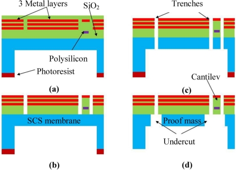
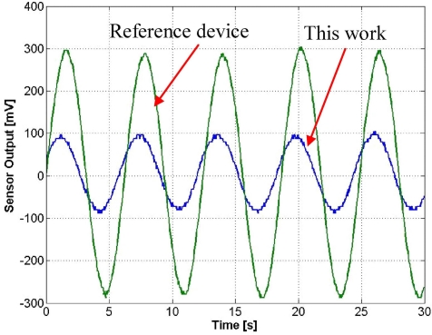
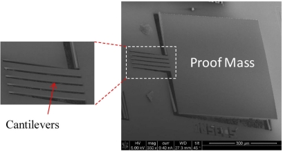
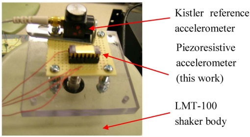
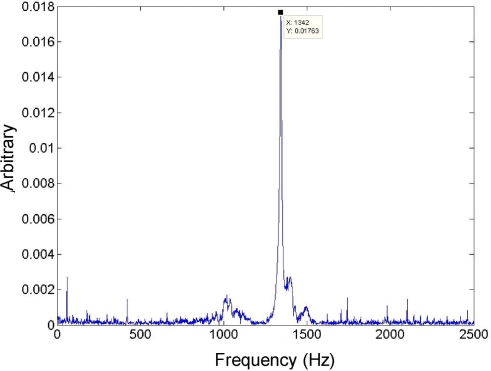
This paper reports a low-cost, high-sensitivity CMOS-MEMS piezoresistive accelerometer with large proof mass. In the device fabricated using ON Semiconductor 0.5 μm CMOS technology, an inherent CMOS polysilicon thin film is utilized as the piezoresistive sensing material. A full Wheatstone bridge was constructed through easy wiring allowed by the three metal layers in the 0.5 μm CMOS technology. The device fabrication process consisted of a standard CMOS process for sensor configuration, and a deep reactive ion etching (DRIE) based post-CMOS microfabrication for MEMS structure release. A bulk single-crystal silicon (SCS) substrate is included in the proof mass to increase sensor sensitivity. In device design and analysis, the self heating of the polysilicon piezoresistors and its effect to the sensor performance is also discussed. With a low operating power of 1.5 mW, the accelerometer demonstrates a sensitivity of 0.077 mV/g prior to any amplification. Dynamic tests have been conducted with a high-end commercial calibrating accelerometer as reference.
本文报道了一种采用低成本、高灵敏度的 CMOS-MEMS 压阻式加速度计,具有较大的质量块。在使用 ON Semiconductor 0.5μm CMOS 技术制造的器件中,采用固有 CMOS 多晶硅薄膜作为压阻式传感材料。通过 0.5μm CMOS 技术中的 3 个金属层允许的简单布线,构建了一个完整的惠斯通电桥。器件制造工艺包括用于传感器配置的标准 CMOS 工艺,以及用于 MEMS 结构释放的基于深反应离子刻蚀(DRIE)的后 CMOS 微加工。在质量块中包含了体单晶硅(SCS)衬底,以提高传感器的灵敏度。在器件设计和分析中,还讨论了多晶硅压阻电阻的自加热及其对传感器性能的影响。该加速度计在 1.5mW 的低工作功率下,在未经任何放大的情况下,灵敏度为 0.077mV/g。采用高端商用校准加速度计作为参考进行了动态测试。