Luo Lin-Bao, Wang Xian-He, Xie Chao, Li Zhong-Jun, Lu Rui, Yang Xiao-Bao, Lu Jian
School of Electronic Science and Applied Physics, Hefei University of Technology, Hefei, Anhui 230009, People's Republic of China ; Department of Mechanical and Biomedical Engineering, City University of Hong Kong, Kowloon, Hong Kong SAR, People's Republic of China.
School of Electronic Science and Applied Physics, Hefei University of Technology, Hefei, Anhui 230009, People's Republic of China.
Nanoscale Res Lett. 2014 Nov 26;9(1):637. doi: 10.1186/1556-276X-9-637. eCollection 2014.
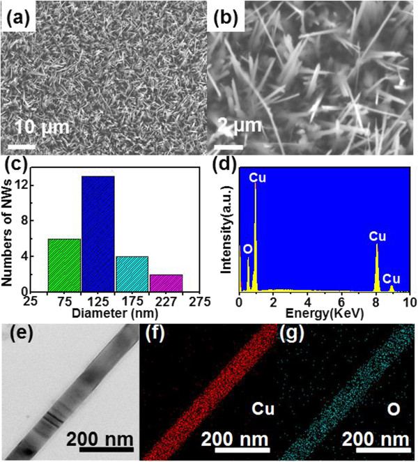
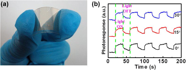
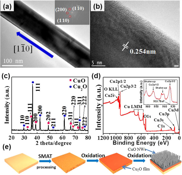
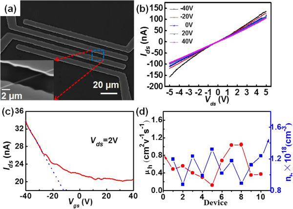
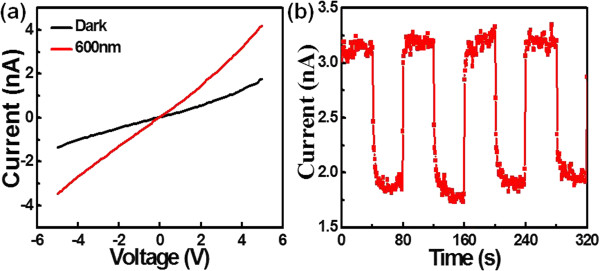
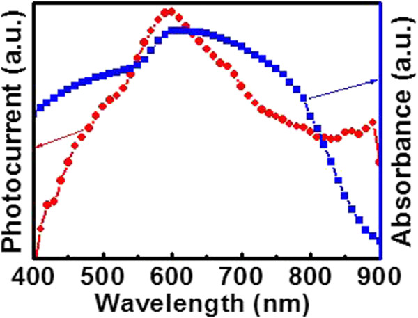
In this work, we presented a surface mechanical attrition treatment (SMAT)-assisted approach to the synthesis of one-dimensional copper oxide nanowires (CuO NWs) for nanodevices applications. The as-prepared CuO NWs have diameter and the length of 50 ~ 200 nm and 5 ~ 20 μm, respectively, with a preferential growth orientation along [1 [Formula: see text] 0] direction. Interestingly, nanofield-effect transistor (nanoFET) based on individual CuO NW exhibited typical p-type electrical conduction, with a hole mobility of 0.129 cm(2)V(-1) s(-1) and hole concentration of 1.34 × 10(18) cm(-3), respectively. According to first-principle calculations, such a p-type electrical conduction behavior was related to the oxygen vacancies in CuO NWs. What is more, the CuO NW device was sensitive to visible light illumination with peak sensitivity at 600 nm. The responsitivity, conductive gain, and detectivity are estimated to be 2.0 × 10(2) A W(-1), 3.95 × 10(2) and 6.38 × 10(11) cm Hz(1/2) W(-1), respectively, which are better than the devices composed of other materials. Further study showed that nanophotodetectors assembled on flexible polyethylene terephthalate (PET) substrate can work under different bending conditions with good reproducibility. The totality of the above results suggests that the present CuO NWs are potential building blocks for assembling high-performance optoelectronic devices.
在这项工作中,我们提出了一种表面机械研磨处理(SMAT)辅助的方法来合成用于纳米器件应用的一维氧化铜纳米线(CuO NWs)。所制备的CuO NWs的直径和长度分别为50200nm和520μm,优先沿[1 [公式:见正文] 0]方向生长。有趣的是,基于单个CuO NW的纳米场效应晶体管(nanoFET)表现出典型的p型导电,空穴迁移率为0.129 cm²V⁻¹ s⁻¹,空穴浓度分别为1.34×10¹⁸ cm⁻³。根据第一性原理计算,这种p型导电行为与CuO NWs中的氧空位有关。此外,CuO NW器件对可见光照射敏感,在600nm处具有峰值灵敏度。响应度、导电增益和探测率估计分别为2.0×10² A W⁻¹、3.95×10²和6.38×10¹¹ cm Hz¹/² W⁻¹,优于由其他材料组成的器件。进一步的研究表明,组装在柔性聚对苯二甲酸乙二醇酯(PET)基板上的纳米光电探测器可以在不同的弯曲条件下工作,且具有良好的可重复性。上述所有结果表明,目前的CuO NWs是组装高性能光电器件的潜在构建块。