• 文献检索
  • 文档翻译
  • 深度研究
  • 学术资讯
  • Suppr Zotero 插件Zotero 插件
  • 邀请有礼
  • 套餐&价格
  • 历史记录
应用&插件
Suppr Zotero 插件Zotero 插件浏览器插件Mac 客户端Windows 客户端微信小程序
定价
高级版会员购买积分包购买API积分包
服务
文献检索文档翻译深度研究API 文档MCP 服务
关于我们
关于 Suppr公司介绍联系我们用户协议隐私条款
关注我们

Suppr 超能文献

核心技术专利:CN118964589B侵权必究
粤ICP备2023148730 号-1Suppr @ 2026

文献检索

告别复杂PubMed语法,用中文像聊天一样搜索,搜遍4000万医学文献。AI智能推荐,让科研检索更轻松。

立即免费搜索

文件翻译

保留排版,准确专业,支持PDF/Word/PPT等文件格式,支持 12+语言互译。

免费翻译文档

深度研究

AI帮你快速写综述,25分钟生成高质量综述,智能提取关键信息,辅助科研写作。

立即免费体验

提高量子亚纳米间隙尖端增强拉曼纳米成像的分辨率。

Improving resolution in quantum subnanometre-gap tip-enhanced Raman nanoimaging.

作者信息

Zhang Yingchao, Voronine Dmitri V, Qiu Shangran, Sinyukov Alexander M, Hamilton Mary, Liege Zachary, Sokolov Alexei V, Zhang Zhenrong, Scully Marlan O

机构信息

Texas A&M University, College Station, TX 77843, USA.

Xi'an Jiaotong University, Xi'an, Shaanxi 710049, China.

出版信息

Sci Rep. 2016 May 25;6:25788. doi: 10.1038/srep25788.

DOI:10.1038/srep25788
PMID:27220882
原文链接:https://pmc.ncbi.nlm.nih.gov/articles/PMC4879532/
Abstract

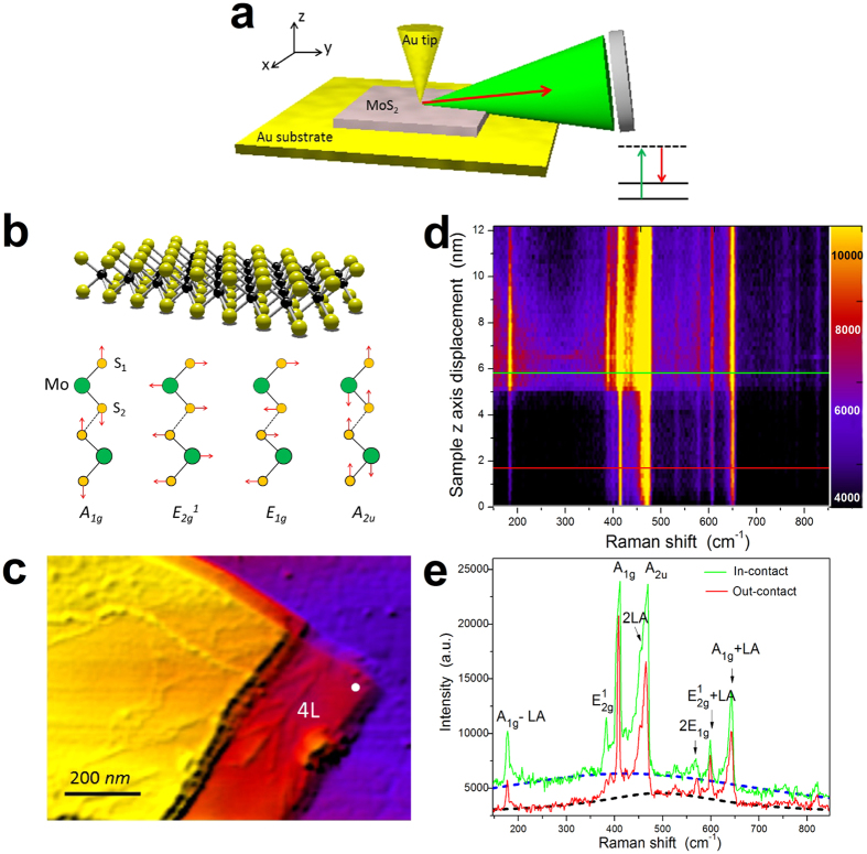
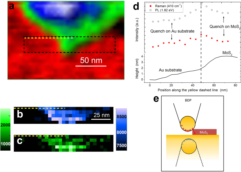
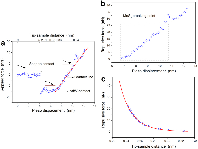
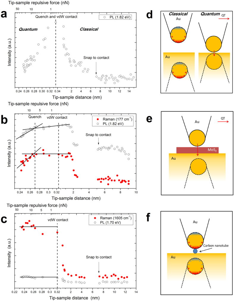
Two-dimensional (2D) materials beyond graphene such as transition metal dichalcogenides (TMDs) have unique mechanical, optical and electronic properties with promising applications in flexible devices, catalysis and sensing. Optical imaging of TMDs using photoluminescence and Raman spectroscopy can reveal the effects of structure, strain, doping, edge states, and surface functionalization from materials to bioscience. However, Raman signals are inherently weak and so far have been limited in spatial resolution in TMDs to a few hundred nanometres which is much larger than the intrinsic scale of these effects. Here we overcome the diffraction limit by using resonant tip-enhanced Raman scattering (TERS) of few-layer MoS2, and obtain nanoscale optical images with ~20 nm spatial resolution. This becomes possible due to electric field enhancement in an optimized subnanometre-gap resonant tip-substrate configuration. We investigate the limits of signal enhancement by varying the tip-sample gap with sub-Angstrom precision and observe a quantum quenching behavior, as well as a Schottky-Ohmic transition, for subnanometre gaps, which enable surface mapping based on this new contrast mechanism. This quantum regime of plasmonic gap-mode enhancement with a few nanometre thick MoS2 junction may be used for designing new quantum optoelectronic devices and sensors with a wide range of applications.

摘要

除石墨烯之外的二维(2D)材料,如过渡金属二硫属化物(TMDs),具有独特的机械、光学和电子特性,在柔性器件、催化和传感等领域有着广阔的应用前景。利用光致发光和拉曼光谱对TMDs进行光学成像,可以揭示从材料到生物科学领域中结构、应变、掺杂、边缘态和表面功能化等方面的影响。然而,拉曼信号本身较弱,到目前为止,TMDs中拉曼信号的空间分辨率仅限于几百纳米,这比这些效应的本征尺度大得多。在这里,我们通过使用少层MoS2的共振针尖增强拉曼散射(TERS)克服了衍射极限,并获得了空间分辨率约为20 nm的纳米级光学图像。这是由于在优化的亚纳米间隙共振针尖 - 基底配置中电场增强才得以实现。我们通过以亚埃精度改变针尖 - 样品间隙来研究信号增强的极限,并观察到对于亚纳米间隙存在量子猝灭行为以及肖特基 - 欧姆转变,这使得基于这种新的对比度机制进行表面映射成为可能。这种具有几纳米厚MoS2结的等离子体间隙模式增强的量子机制可用于设计具有广泛应用的新型量子光电器件和传感器。

https://cdn.ncbi.nlm.nih.gov/pmc/blobs/4325/4879532/994c1d7e354a/srep25788-f4.jpg
https://cdn.ncbi.nlm.nih.gov/pmc/blobs/4325/4879532/2d486fb68bba/srep25788-f1.jpg
https://cdn.ncbi.nlm.nih.gov/pmc/blobs/4325/4879532/1bb1f04dd169/srep25788-f2.jpg
https://cdn.ncbi.nlm.nih.gov/pmc/blobs/4325/4879532/4dfef80ae932/srep25788-f3.jpg
https://cdn.ncbi.nlm.nih.gov/pmc/blobs/4325/4879532/994c1d7e354a/srep25788-f4.jpg

相似文献

1
Improving resolution in quantum subnanometre-gap tip-enhanced Raman nanoimaging.提高量子亚纳米间隙尖端增强拉曼纳米成像的分辨率。
Sci Rep. 2016 May 25;6:25788. doi: 10.1038/srep25788.
2
Transition metal dichalcogenides and beyond: synthesis, properties, and applications of single- and few-layer nanosheets.过渡金属二卤化物及其以外的单层和少层纳米片的合成、性质和应用。
Acc Chem Res. 2015 Jan 20;48(1):56-64. doi: 10.1021/ar5002846. Epub 2014 Dec 9.
3
Nanoscale mapping of intrinsic defects in single-layer graphene using tip-enhanced Raman spectroscopy.利用针尖增强拉曼光谱对单层石墨烯中的本征缺陷进行纳米级成像。
Chem Commun (Camb). 2016 Jul 7;52(53):8227-30. doi: 10.1039/c6cc01990k. Epub 2016 Jun 9.
4
Comparative study of Raman spectroscopy in graphene and MoS2-type transition metal dichalcogenides.石墨烯和 MoS2 型过渡金属二卤代物的拉曼光谱比较研究。
Acc Chem Res. 2015 Jan 20;48(1):41-7. doi: 10.1021/ar500280m. Epub 2014 Dec 9.
5
Giant gap-plasmon tip-enhanced Raman scattering of MoS monolayers on Au nanocluster arrays.金纳米团簇阵列上的 MoS 单层的巨间隙等离子体尖端增强拉曼散射。
Nanoscale. 2018 Feb 8;10(6):2755-2763. doi: 10.1039/c7nr06640f.
6
Resonant Raman scattering on graphene: SERS and gap-mode TERS.石墨烯上的共振拉曼散射:表面增强拉曼散射和能隙模式针尖增强拉曼光谱
RSC Adv. 2024 Jan 23;14(6):3667-3674. doi: 10.1039/d3ra07018b.
7
Surface- and Tip-Enhanced Raman Scattering by CdSe Nanocrystals on Plasmonic Substrates.等离子体基底上CdSe纳米晶体的表面和尖端增强拉曼散射
Nanomaterials (Basel). 2022 Jun 26;12(13):2197. doi: 10.3390/nano12132197.
8
Coupling nanobubbles in 2D lateral heterostructures.二维横向异质结构中的耦合纳米气泡
Nanoscale. 2022 Jun 9;14(22):8050-8059. doi: 10.1039/d2nr00512c.
9
Highly Localized Strain in a MoS/Au Heterostructure Revealed by Tip-Enhanced Raman Spectroscopy.由针尖增强拉曼光谱揭示的 MoS/Au 异质结构中的高度局域应变。
Nano Lett. 2017 Oct 11;17(10):6027-6033. doi: 10.1021/acs.nanolett.7b02322. Epub 2017 Sep 25.
10
Transition metal chalcogenides: ultrathin inorganic materials with tunable electronic properties.过渡金属硫属化物:具有可调电子性质的超薄无机材料。
Acc Chem Res. 2015 Jan 20;48(1):65-72. doi: 10.1021/ar500277z. Epub 2014 Dec 9.

引用本文的文献

1
Classical vs. quantum plasmon-induced molecular transformations at metallic nanojunctions.金属纳米结处经典与量子等离激元诱导的分子转变
Proc Natl Acad Sci U S A. 2024 Apr 2;121(14):e2319233121. doi: 10.1073/pnas.2319233121. Epub 2024 Mar 28.
2
Tunable interlayer excitons and switchable interlayer trions via dynamic near-field cavity.通过动态近场腔实现的可调层间激子和可切换层间三重态激子
Light Sci Appl. 2023 Mar 3;12(1):59. doi: 10.1038/s41377-023-01087-5.
3
Resonant tip-enhanced Raman scattering by CdSe nanocrystals on plasmonic substrates.

本文引用的文献

1
Recent Advances in Tip-Enhanced Raman Spectroscopy.针尖增强拉曼光谱学的最新进展
J Phys Chem Lett. 2014 Sep 18;5(18):3125-30. doi: 10.1021/jz5015746. Epub 2014 Aug 29.
2
Visualizing nanoscale excitonic relaxation properties of disordered edges and grain boundaries in monolayer molybdenum disulfide.可视化单层二硫化钼中无序边缘和晶界的纳米级激子弛豫特性。
Nat Commun. 2015 Aug 13;6:7993. doi: 10.1038/ncomms8993.
3
Tip-enhanced Raman mapping of local strain in graphene.石墨烯中局部应变的针尖增强拉曼映射
CdSe纳米晶体在等离子体基底上的共振针尖增强拉曼散射。
Nanoscale Adv. 2020 Oct 7;2(11):5441-5449. doi: 10.1039/d0na00554a. eCollection 2020 Nov 11.
4
A reclaimed piezoelectric catalyst of MoS@TNr composites as high-performance anode materials for supercapacitors.一种作为超级电容器高性能阳极材料的MoS@TNr复合材料回收压电催化剂。
RSC Adv. 2020 Oct 22;10(63):38715-38726. doi: 10.1039/d0ra06532c. eCollection 2020 Oct 15.
5
Probing stacking configurations in a few layered MoS by low frequency Raman spectroscopy.通过低频拉曼光谱探测几层MoS中的堆叠构型
Sci Rep. 2020 Dec 4;10(1):21227. doi: 10.1038/s41598-020-78238-w.
6
Infrared and Raman chemical imaging and spectroscopy at the nanoscale.纳米尺度的红外和拉曼化学成像与光谱学。
Chem Soc Rev. 2020 Jun 7;49(11):3315-3347. doi: 10.1039/c8cs00916c. Epub 2020 May 19.
7
Quantum plasmonic control of trions in a picocavity with monolayer WS.在具有单层 WS 的微腔中控制量子等离子激元中的三体子
Sci Adv. 2019 Oct 11;5(10):eaau8763. doi: 10.1126/sciadv.aau8763. eCollection 2019 Oct.
8
Spectroscopic Imaging at the Nanoscale: Technologies and Recent Applications.纳米级光谱成像:技术与近期应用
Anal Chem. 2018 Jan 2;90(1):440-458. doi: 10.1021/acs.analchem.7b04151. Epub 2017 Oct 27.
Nanotechnology. 2015 May 1;26(17):175702. doi: 10.1088/0957-4484/26/17/175702. Epub 2015 Apr 2.
4
Three-fold rotational defects in two-dimensional transition metal dichalcogenides.二维过渡金属二硫属化物中的三重旋转缺陷
Nat Commun. 2015 Apr 2;6:6736. doi: 10.1038/ncomms7736.
5
Comparative Study of Potential Applications of Graphene, MoS2, and Other Two-Dimensional Materials in Energy Devices, Sensors, and Related Areas.石墨烯、二硫化钼及其他二维材料在能源器件、传感器及相关领域潜在应用的比较研究
ACS Appl Mater Interfaces. 2015 Apr 22;7(15):7809-32. doi: 10.1021/am509096x. Epub 2015 Apr 9.
6
Exploring atomic defects in molybdenum disulphide monolayers.探索二硫化钼单层中的原子缺陷。
Nat Commun. 2015 Feb 19;6:6293. doi: 10.1038/ncomms7293.
7
Bandgap tunability at single-layer molybdenum disulphide grain boundaries.单层二硫化钼晶界的带隙可调谐性。
Nat Commun. 2015 Feb 17;6:6298. doi: 10.1038/ncomms7298.
8
Phonon and Raman scattering of two-dimensional transition metal dichalcogenides from monolayer, multilayer to bulk material.二维过渡金属二卤族化合物的声子和拉曼散射:从单层、多层到体材料。
Chem Soc Rev. 2015 May 7;44(9):2757-85. doi: 10.1039/c4cs00282b. Epub 2015 Feb 13.
9
Single-layer MoS2 electronics.单层 MoS2 电子学。
Acc Chem Res. 2015 Jan 20;48(1):100-10. doi: 10.1021/ar500274q. Epub 2015 Jan 2.
10
Comparative study of Raman spectroscopy in graphene and MoS2-type transition metal dichalcogenides.石墨烯和 MoS2 型过渡金属二卤代物的拉曼光谱比较研究。
Acc Chem Res. 2015 Jan 20;48(1):41-7. doi: 10.1021/ar500280m. Epub 2014 Dec 9.