State Key Laboratory of Functional Materials for Informatics, Shanghai Institute of Microsystem and Information Technology, Chinese Academy of Sciences, 865 Changning Road, Shanghai 200050, China.
School of Physical Science and Technology, ShanghaiTech University, 319 Yueyang Road, Shanghai 200031, China.
Nat Commun. 2017 Mar 9;8:14703. doi: 10.1038/ncomms14703.
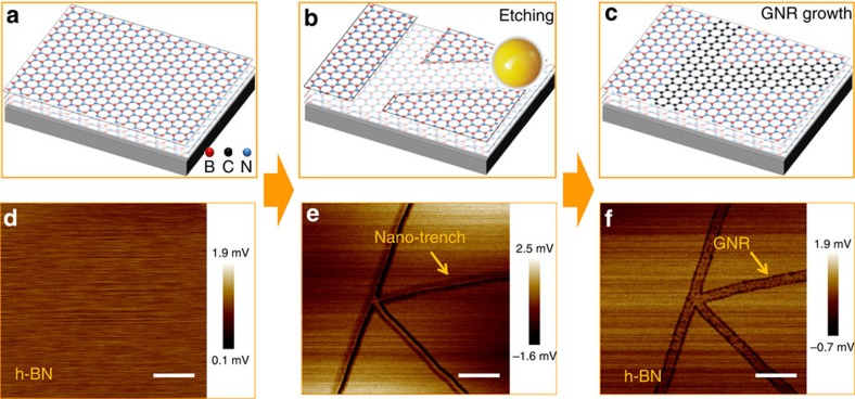
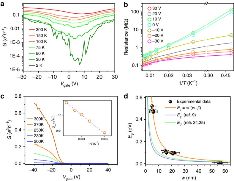
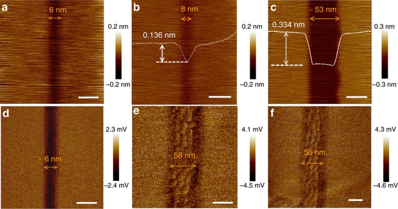
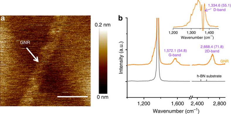
Graphene nanoribbons (GNRs) are ultra-narrow strips of graphene that have the potential to be used in high-performance graphene-based semiconductor electronics. However, controlled growth of GNRs on dielectric substrates remains a challenge. Here, we report the successful growth of GNRs directly on hexagonal boron nitride substrates with smooth edges and controllable widths using chemical vapour deposition. The approach is based on a type of template growth that allows for the in-plane epitaxy of mono-layered GNRs in nano-trenches on hexagonal boron nitride with edges following a zigzag direction. The embedded GNR channels show excellent electronic properties, even at room temperature. Such in-plane hetero-integration of GNRs, which is compatible with integrated circuit processing, creates a gapped channel with a width of a few benzene rings, enabling the development of digital integrated circuitry based on GNRs.
石墨烯纳米带(GNRs)是石墨烯的超窄条带,有望用于高性能基于石墨烯的半导体电子学。然而,在介电衬底上控制 GNRs 的生长仍然是一个挑战。在这里,我们报告了使用化学气相沉积法直接在具有平滑边缘和可控宽度的六方氮化硼衬底上成功生长 GNRs。该方法基于一种模板生长方法,允许在具有锯齿状边缘的六方氮化硼纳米槽中进行单层 GNRs 的面内外延。嵌入的 GNR 沟道表现出优异的电子性能,即使在室温下也是如此。这种与集成电路处理兼容的 GNRs 的面内异质集成,形成了一个具有几个苯环宽度的带隙沟道,从而能够开发基于 GNRs 的数字集成电路。