• 文献检索
  • 文档翻译
  • 深度研究
  • 学术资讯
  • Suppr Zotero 插件Zotero 插件
  • 邀请有礼
  • 套餐&价格
  • 历史记录
应用&插件
Suppr Zotero 插件Zotero 插件浏览器插件Mac 客户端Windows 客户端微信小程序
定价
高级版会员购买积分包购买API积分包
服务
文献检索文档翻译深度研究API 文档MCP 服务
关于我们
关于 Suppr公司介绍联系我们用户协议隐私条款
关注我们

Suppr 超能文献

核心技术专利:CN118964589B侵权必究
粤ICP备2023148730 号-1Suppr @ 2026

文献检索

告别复杂PubMed语法,用中文像聊天一样搜索,搜遍4000万医学文献。AI智能推荐,让科研检索更轻松。

立即免费搜索

文件翻译

保留排版,准确专业,支持PDF/Word/PPT等文件格式,支持 12+语言互译。

免费翻译文档

深度研究

AI帮你快速写综述,25分钟生成高质量综述,智能提取关键信息,辅助科研写作。

立即免费体验

通过扫描电子纳米衍射记录的大型衍射数据集确定三维纳米结构。

Three-dimensional nanostructure determination from a large diffraction data set recorded using scanning electron nanodiffraction.

作者信息

Meng Yifei, Zuo Jian-Min

机构信息

Department of Materials Science and Engineering, University of Illinois at Urbana-Champaign, 1304 W. Green Street, Urbana, IL 61801, USA.

Fredrick Seitz Materials Research Laboratory, University of Illinois at Urbana-Champaign, 104 S. Goodwin Avenue, Urbana, IL 61801, USA.

出版信息

IUCrJ. 2016 Jul 4;3(Pt 5):300-308. doi: 10.1107/S205225251600943X. eCollection 2016 Sep 1.

DOI:10.1107/S205225251600943X
PMID:28461891
原文链接:https://pmc.ncbi.nlm.nih.gov/articles/PMC5391852/
Abstract

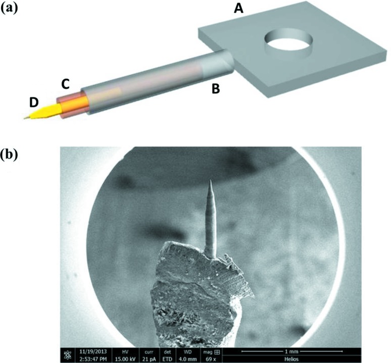
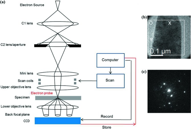
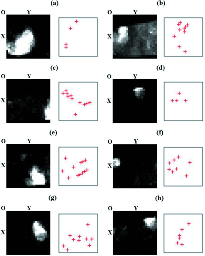
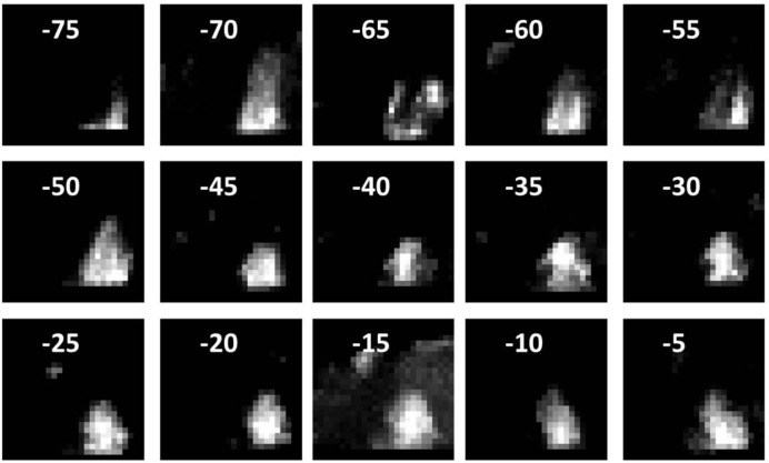
A diffraction-based technique is developed for the determination of three-dimensional nanostructures. The technique employs high-resolution and low-dose scanning electron nanodiffraction (SEND) to acquire three-dimensional diffraction patterns, with the help of a special sample holder for large-angle rotation. Grains are identified in three-dimensional space based on crystal orientation and on reconstructed dark-field images from the recorded diffraction patterns. Application to a nanocrystalline TiN thin film shows that the three-dimensional morphology of columnar TiN grains of tens of nanometres in diameter can be reconstructed using an algebraic iterative algorithm under specified prior conditions, together with their crystallographic orientations. The principles can be extended to multiphase nanocrystalline materials as well. Thus, the tomographic SEND technique provides an effective and adaptive way of determining three-dimensional nanostructures.

摘要

一种基于衍射的技术被开发用于确定三维纳米结构。该技术采用高分辨率和低剂量扫描电子纳米衍射(SEND)来获取三维衍射图案,借助一个用于大角度旋转的特殊样品架。基于晶体取向以及从记录的衍射图案重建的暗场图像,在三维空间中识别晶粒。应用于纳米晶TiN薄膜表明,在特定的先验条件下,使用代数迭代算法可以重建直径为数十纳米的柱状TiN晶粒的三维形态及其晶体学取向。这些原理也可以扩展到多相纳米晶材料。因此,断层扫描SEND技术为确定三维纳米结构提供了一种有效且自适应的方法。

https://cdn.ncbi.nlm.nih.gov/pmc/blobs/b0ea/5391852/301b44785953/m-03-00300-fig6.jpg
https://cdn.ncbi.nlm.nih.gov/pmc/blobs/b0ea/5391852/24363c34dd4e/m-03-00300-fig1.jpg
https://cdn.ncbi.nlm.nih.gov/pmc/blobs/b0ea/5391852/655ce67482d8/m-03-00300-fig2.jpg
https://cdn.ncbi.nlm.nih.gov/pmc/blobs/b0ea/5391852/eab0ac330005/m-03-00300-fig3.jpg
https://cdn.ncbi.nlm.nih.gov/pmc/blobs/b0ea/5391852/da3c62d5c42c/m-03-00300-fig4.jpg
https://cdn.ncbi.nlm.nih.gov/pmc/blobs/b0ea/5391852/d71caed8c6c9/m-03-00300-fig5.jpg
https://cdn.ncbi.nlm.nih.gov/pmc/blobs/b0ea/5391852/301b44785953/m-03-00300-fig6.jpg

相似文献

1
Three-dimensional nanostructure determination from a large diffraction data set recorded using scanning electron nanodiffraction.通过扫描电子纳米衍射记录的大型衍射数据集确定三维纳米结构。
IUCrJ. 2016 Jul 4;3(Pt 5):300-308. doi: 10.1107/S205225251600943X. eCollection 2016 Sep 1.
2
TEM based high resolution and low-dose scanning electron nanodiffraction technique for nanostructure imaging and analysis.基于透射电子显微镜的高分辨率低剂量扫描电子纳米衍射技术用于纳米结构成像与分析。
Micron. 2015 Apr;71:39-45. doi: 10.1016/j.micron.2015.01.002. Epub 2015 Jan 19.
3
Nanocrystal segmentation in scanning precession electron diffraction data.扫描进动电子衍射数据中的纳米晶体分割
J Microsc. 2020 Sep;279(3):158-167. doi: 10.1111/jmi.12850. Epub 2019 Dec 9.
4
Diffraction imaging of nanocrystalline structures in organic semiconductor molecular thin films.有机半导体分子薄膜中纳米晶体结构的衍射成像
Nat Mater. 2019 Aug;18(8):860-865. doi: 10.1038/s41563-019-0387-3. Epub 2019 Jun 3.
5
Crystallographic Orientation Analysis of Nanocrystalline Tungsten Thin Film Using TEM Precession Electron Diffraction and SEM Transmission Kikuchi Diffraction.利用透射电子显微镜进动电子衍射和扫描电子显微镜透射菊池衍射对纳米晶钨薄膜进行晶体取向分析。
Microsc Microanal. 2021 Apr;27(2):237-249. doi: 10.1017/S1431927621000027.
6
Three-dimensional EBSD study on the relationship between triple junctions and columnar grains in electrodeposited Co-Ni films.电沉积Co-Ni薄膜中三叉晶界与柱状晶粒关系的三维电子背散射衍射研究
J Microsc. 2008 Jun;230(Pt 3):487-98. doi: 10.1111/j.1365-2818.2008.02008.x.
7
Four-Dimensional Scanning Transmission Electron Microscopy (4D-STEM): From Scanning Nanodiffraction to Ptychography and Beyond.四维扫描透射电子显微镜(4D-STEM):从扫描纳米衍射到叠层成像及其他
Microsc Microanal. 2019 Jun;25(3):563-582. doi: 10.1017/S1431927619000497. Epub 2019 May 14.
8
Reconstructing dual-phase nanometer scale grains within a pearlitic steel tip in 3D through 4D-scanning precession electron diffraction tomography and automated crystal orientation mapping.通过四维扫描进动电子衍射断层扫描和自动晶体取向映射在三维空间中重建珠光体钢尖端内的双相纳米尺度晶粒。
Ultramicroscopy. 2022 Aug;238:113536. doi: 10.1016/j.ultramic.2022.113536. Epub 2022 Apr 27.
9
Automated Crystal Orientation Mapping in py4DSTEM using Sparse Correlation Matching.在py4DSTEM中使用稀疏相关匹配的自动晶体取向映射
Microsc Microanal. 2022 Feb 9:1-14. doi: 10.1017/S1431927622000101.
10
Nanometres-resolution Kikuchi patterns from materials science specimens with transmission electron forward scatter diffraction in the scanning electron microscope.利用扫描电子显微镜中的透射电子前向散射衍射技术,从材料科学样品中获得纳米分辨率的菊池花样。
J Microsc. 2013 Apr;250(1):1-14. doi: 10.1111/jmi.12007. Epub 2013 Jan 24.

引用本文的文献

1
Correlating Grain Boundary Character and Composition in 3-Dimensions Using 4D-Scanning Precession Electron Diffraction and Atom Probe Tomography.使用4D扫描进动电子衍射和原子探针断层扫描技术在三维空间中关联晶界特征与成分
Small Methods. 2025 May;9(5):e2401650. doi: 10.1002/smtd.202401650. Epub 2025 Feb 28.
2
Spinel oxide enables high-temperature self-lubrication in superalloys.尖晶石氧化物使高温合金具备高温自润滑性能。
Nat Commun. 2024 Nov 20;15(1):10039. doi: 10.1038/s41467-024-54482-w.
3
Atomic structures determined from digitally defined nanocrystalline regions.

本文引用的文献

1
Scanning precession electron tomography for three-dimensional nanoscale orientation imaging and crystallographic analysis.用于三维纳米级取向成像和晶体学分析的扫描进动电子断层扫描术。
Nat Commun. 2015 Jun 1;6:7267. doi: 10.1038/ncomms8267.
2
TEM based high resolution and low-dose scanning electron nanodiffraction technique for nanostructure imaging and analysis.基于透射电子显微镜的高分辨率低剂量扫描电子纳米衍射技术用于纳米结构成像与分析。
Micron. 2015 Apr;71:39-45. doi: 10.1016/j.micron.2015.01.002. Epub 2015 Jan 19.
3
Precession electron diffraction - a topical review.
由数字定义的纳米晶区域确定的原子结构。
IUCrJ. 2020 Apr 10;7(Pt 3):490-499. doi: 10.1107/S2052252520004030. eCollection 2020 May 1.
4
Dynamic-template-directed multiscale assembly for large-area coating of highly-aligned conjugated polymer thin films.动态模板导向的多尺度组装方法用于大面积涂覆高度取向的共轭聚合物薄膜。
Nat Commun. 2017 Jul 13;8:16070. doi: 10.1038/ncomms16070.
5
Developments in the structural science of materials.材料结构科学的发展。
IUCrJ. 2017 Apr 25;4(Pt 3):199-201. doi: 10.1107/S2052252517006145. eCollection 2017 May 1.
进动电子衍射——一篇专题综述。
IUCrJ. 2015 Jan 1;2(Pt 1):126-36. doi: 10.1107/S2052252514022283.
4
Atomic-scale quantification of grain boundary segregation in nanocrystalline material.纳米晶材料中晶界偏析的原子尺度定量。
Phys Rev Lett. 2014 Mar 28;112(12):126103. doi: 10.1103/PhysRevLett.112.126103. Epub 2014 Mar 27.
5
Orientation precision of TEM-based orientation mapping techniques.基于 TEM 的取向映射技术的取向精度。
Ultramicroscopy. 2014 Jan;136:107-18. doi: 10.1016/j.ultramic.2013.08.008. Epub 2013 Aug 30.
6
Lattice and strain analysis of atomic resolution Z-contrast images based on template matching.基于模板匹配的原子分辨 Z 衬度像的晶格和应变分析。
Ultramicroscopy. 2014 Jan;136:50-60. doi: 10.1016/j.ultramic.2013.07.018. Epub 2013 Aug 7.
7
Grain boundary character distribution of nanocrystalline Cu thin films using stereological analysis of transmission electron microscope orientation maps.利用透射电子显微镜取向图的体视学分析研究纳米晶 Cu 薄膜的晶界特征分布。
Microsc Microanal. 2013 Feb;19(1):111-9. doi: 10.1017/S1431927612014055.
8
Nanostructured metal chalcogenides: synthesis, modification, and applications in energy conversion and storage devices.纳米结构金属硫族化合物:在能量转换和存储装置中的合成、修饰及应用。
Chem Soc Rev. 2013 Apr 7;42(7):2986-3017. doi: 10.1039/c2cs35310e.
9
Three-dimensional orientation mapping in the transmission electron microscope.透射电子显微镜中的三维取向映射。
Science. 2011 May 13;332(6031):833-4. doi: 10.1126/science.1202202.
10
Ordered mesoporous alpha-MoO3 with iso-oriented nanocrystalline walls for thin-film pseudocapacitors.有序介孔 α-MoO3 具有各向同性纳米晶壁,用于薄膜赝电容器。
Nat Mater. 2010 Feb;9(2):146-51. doi: 10.1038/nmat2612. Epub 2010 Jan 10.