Zernike Institute for Advanced Materials, University of Groningen , Nijenborgh 4, Groningen 9747AG, The Netherlands.
Department of Advanced Materials Science, School of Frontier Sciences, The University of Tokyo , 5-1-5 Kashiwanoha, Kashiwa, Chiba 277-8561, Japan.
ACS Appl Mater Interfaces. 2017 May 31;9(21):18039-18045. doi: 10.1021/acsami.7b02867. Epub 2017 May 16.
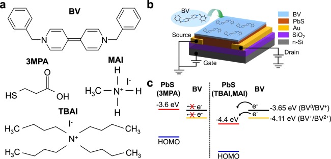
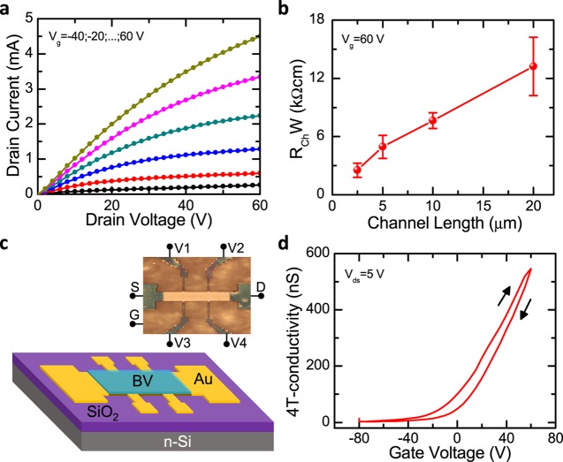
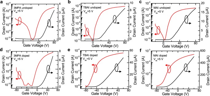
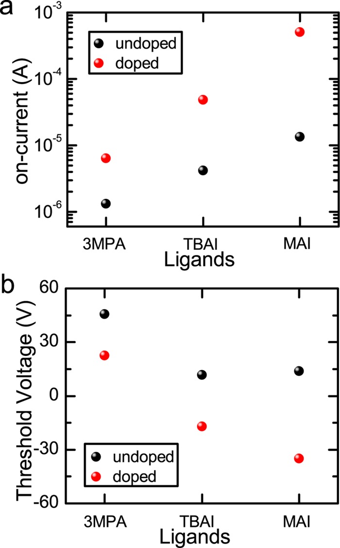
PbS quantum dots (QDs) are remarkable semiconducting materials, which are compatible with low-cost solution-processed electronic device fabrication. Understanding the doping of these materials is one of the great research interests, as it is a necessary step to improve the device performance as well as to enhance the applicability of this system for diverse optoelectronic applications. Here, we report the efficient doping of the PbS QD films with the use of solution-processable organic molecules. By engineering the energy levels of the donor molecules and the PbS QDs through the use of different cross-linking ligands, we are able to control the characteristics of PbS field-effect transistors (FETs) from ambipolar to strongly n-type. Because the doping promotes trap filling, the charge carrier mobility is improved up to 0.64 cm V s, which is the highest mobility reported for low-temperature processed PbS FETs employing SiO as the gate dielectric. The doping also reduces the contact resistance of the devices, which can also explain the origin of the increased mobility.
PbS 量子点 (QDs) 是一种卓越的半导体材料,与低成本的溶液处理电子器件制造工艺兼容。了解这些材料的掺杂是一个重要的研究兴趣,因为这是提高器件性能以及增强该体系在各种光电应用中的适用性的必要步骤。在这里,我们报告了使用可溶液处理的有机分子对 PbS QD 薄膜进行高效掺杂。通过工程化施主分子和 PbS QD 的能级,使用不同的交联配体,我们能够控制 PbS 场效应晶体管 (FET) 的特性,从双极性到强 n 型。由于掺杂促进了陷阱填充,电荷载流子迁移率提高到 0.64 cm V s,这是使用 SiO2 作为栅介质的低温处理 PbS FET 中报道的最高迁移率。掺杂还降低了器件的接触电阻,这也可以解释迁移率提高的原因。