• 文献检索
  • 文档翻译
  • 深度研究
  • 学术资讯
  • Suppr Zotero 插件Zotero 插件
  • 邀请有礼
  • 套餐&价格
  • 历史记录
应用&插件
Suppr Zotero 插件Zotero 插件浏览器插件Mac 客户端Windows 客户端微信小程序
定价
高级版会员购买积分包购买API积分包
服务
文献检索文档翻译深度研究API 文档MCP 服务
关于我们
关于 Suppr公司介绍联系我们用户协议隐私条款
关注我们

Suppr 超能文献

核心技术专利:CN118964589B侵权必究
粤ICP备2023148730 号-1Suppr @ 2026

文献检索

告别复杂PubMed语法,用中文像聊天一样搜索,搜遍4000万医学文献。AI智能推荐,让科研检索更轻松。

立即免费搜索

文件翻译

保留排版,准确专业,支持PDF/Word/PPT等文件格式,支持 12+语言互译。

免费翻译文档

深度研究

AI帮你快速写综述,25分钟生成高质量综述,智能提取关键信息,辅助科研写作。

立即免费体验

通过隧道摩擦带电实现二维电子的可重写幽灵浮栅

Rewritable ghost floating gates by tunnelling triboelectrification for two-dimensional electronics.

机构信息

School of Advanced Materials Science and Engineering, Sungkyunkwan University (SKKU), 2066 Seobu-ro, Jangan-gu, Suwon, Gyeonggi-do 440-746, Republic of Korea.

SKKU Advanced Institute of Nanotechnology, Sungkyunkwan University (SKKU), Suwon 440-746, Republic of Korea.

出版信息

Nat Commun. 2017 Jun 26;8:15891. doi: 10.1038/ncomms15891.

DOI:10.1038/ncomms15891
PMID:28649986
原文链接:https://pmc.ncbi.nlm.nih.gov/articles/PMC5490184/
Abstract

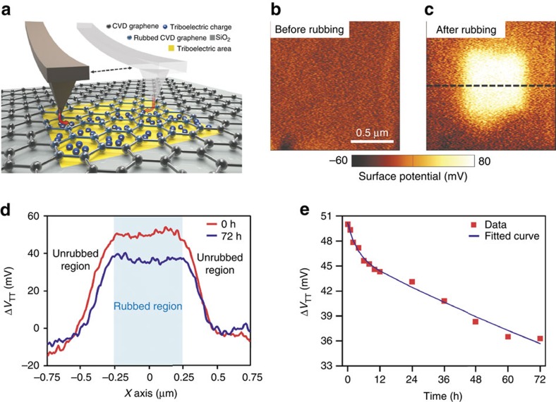
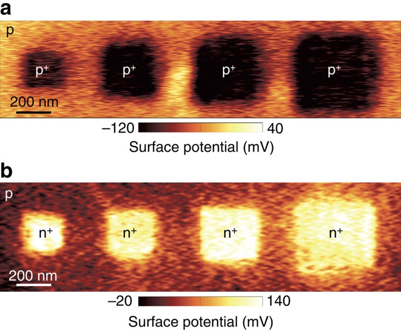
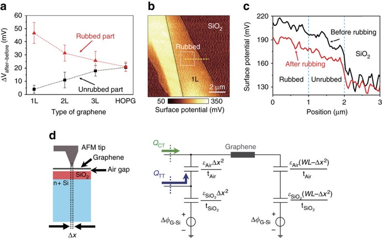
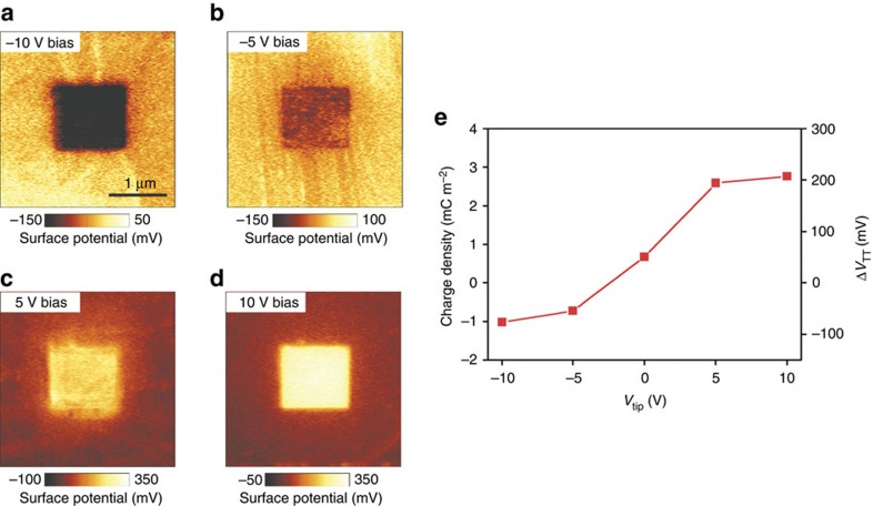
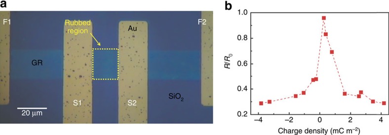
Gates can electrostatically control charges inside two-dimensional materials. However, integrating independent gates typically requires depositing and patterning suitable insulators and conductors. Moreover, after manufacturing, gates are unchangeable. Here we introduce tunnelling triboelectrification for localizing electric charges in very close proximity of two-dimensional materials. As representative materials, we use chemical vapour deposition graphene deposited on a SiO/Si substrate. The triboelectric charges, generated by friction with a Pt-coated atomic force microscope tip and injected through defects, are trapped at the air-SiO interface underneath graphene and act as ghost floating gates. Tunnelling triboelectrification uniquely permits to create, modify and destroy p and n regions at will with the spatial resolution of atomic force microscopes. As a proof of concept, we draw rewritable p/n and p/p junctions with resolutions as small as 200 nm. Our results open the way to time-variant two-dimensional electronics where conductors, p and n regions can be defined on demand.

摘要

盖茨可以静电控制二维材料内部的电荷。然而,集成独立的栅极通常需要沉积和图案化合适的绝缘体和导体。此外,制造后,栅极是不可改变的。在这里,我们引入隧道摩擦带电现象,以便在二维材料非常接近的地方定位电荷。作为代表性材料,我们使用化学气相沉积法在 SiO/Si 衬底上沉积的石墨烯。通过与涂有 Pt 的原子力显微镜尖端的摩擦产生的摩擦电荷,并通过缺陷注入,被捕获在石墨烯下方的空气-SiO 界面处,并充当幽灵浮栅。隧道摩擦带电现象独特地允许以原子力显微镜的空间分辨率随意创建、修改和破坏 p 和 n 区。作为概念验证,我们用分辨率低至 200nm 的重写 p/n 和 p/p 结。我们的结果为时变二维电子学开辟了道路,其中可以根据需要定义导体、p 和 n 区。

https://cdn.ncbi.nlm.nih.gov/pmc/blobs/af9e/5490184/b36633799c25/ncomms15891-f5.jpg
https://cdn.ncbi.nlm.nih.gov/pmc/blobs/af9e/5490184/a75e32604668/ncomms15891-f1.jpg
https://cdn.ncbi.nlm.nih.gov/pmc/blobs/af9e/5490184/50c3ac64dff9/ncomms15891-f2.jpg
https://cdn.ncbi.nlm.nih.gov/pmc/blobs/af9e/5490184/b2756f6c64ea/ncomms15891-f3.jpg
https://cdn.ncbi.nlm.nih.gov/pmc/blobs/af9e/5490184/93c66c32572f/ncomms15891-f4.jpg
https://cdn.ncbi.nlm.nih.gov/pmc/blobs/af9e/5490184/b36633799c25/ncomms15891-f5.jpg

相似文献

1
Rewritable ghost floating gates by tunnelling triboelectrification for two-dimensional electronics.通过隧道摩擦带电实现二维电子的可重写幽灵浮栅
Nat Commun. 2017 Jun 26;8:15891. doi: 10.1038/ncomms15891.
2
Nanoscale charge transfer and diffusion at the MoS/SiO interface by atomic force microscopy: contact injection versus triboelectrification.通过原子力显微镜研究MoS/SiO界面处的纳米级电荷转移与扩散:接触注入与摩擦起电
Nanotechnology. 2018 Aug 31;29(35):355701. doi: 10.1088/1361-6528/aacad7. Epub 2018 Jun 6.
3
Controllable Tunneling Triboelectrification of Two-Dimensional Chemical Vapor Deposited MoS.二维化学气相沉积MoS₂的可控隧道摩擦起电
Sci Rep. 2019 Jan 23;9(1):334. doi: 10.1038/s41598-018-36830-1.
4
Nanoscale triboelectrification gated transistor.纳米级摩擦起电门控晶体管。
Nat Commun. 2020 Feb 26;11(1):1054. doi: 10.1038/s41467-020-14909-6.
5
Triboelectrification of Two-Dimensional Chemical Vapor Deposited WS at Nanoscale.二维化学气相沉积WS在纳米尺度下的摩擦起电
Sci Rep. 2019 Aug 29;9(1):12570. doi: 10.1038/s41598-019-49107-y.
6
In situ quantitative study of nanoscale triboelectrification and patterning.纳米尺度摩擦带电和图案化的原位定量研究。
Nano Lett. 2013 Jun 12;13(6):2771-6. doi: 10.1021/nl401006x. Epub 2013 May 1.
7
Transfer free graphene growth on SiO substrate at 250 °C.在 250°C 的 SiO 衬底上无载体石墨烯生长。
Sci Rep. 2017 Mar 2;7:43756. doi: 10.1038/srep43756.
8
Control of Triboelectrification by Engineering Surface Dipole and Surface Electronic State.通过工程表面偶极子和表面电子态控制摩擦起电。
ACS Appl Mater Interfaces. 2016 Jul 20;8(28):18519-25. doi: 10.1021/acsami.6b02802. Epub 2016 Jul 5.
9
Enhanced High-Resolution Triboelectrification-Induced Electroluminescence for Self-Powered Visualized Interactive Sensing.用于自供电可视化交互传感的增强型高分辨率摩擦起电致发光
ACS Appl Mater Interfaces. 2019 Apr 10;11(14):13796-13802. doi: 10.1021/acsami.9b02313. Epub 2019 Mar 28.
10
Flexible integrated circuits and multifunctional electronics based on single atomic layers of MoS2 and graphene.基于二硫化钼和石墨烯单原子层的柔性集成电路及多功能电子器件。
Nanotechnology. 2015 Mar 20;26(11):115202. doi: 10.1088/0957-4484/26/11/115202. Epub 2015 Feb 24.

引用本文的文献

1
Reversible and controllable reduction in friction of atomically thin two-dimensional materials through high-stress pre-rubbing.通过高应力预摩擦实现原子级薄二维材料摩擦的可逆和可控降低。
Nat Commun. 2024 Nov 15;15(1):9897. doi: 10.1038/s41467-024-54363-2.
2
Highly efficient microbial inactivation enabled by tunneling charges injected through two-dimensional electronics.通过二维电子注入的隧穿电荷实现高效微生物灭活。
Sci Adv. 2024 May 3;10(18):eadl5067. doi: 10.1126/sciadv.adl5067.
3
Recent Advances in Triboelectric Nanogenerators: From Technological Progress to Commercial Applications.

本文引用的文献

1
Silicene field-effect transistors operating at room temperature.硅烯室温下的场效应晶体管。
Nat Nanotechnol. 2015 Mar;10(3):227-31. doi: 10.1038/nnano.2014.325. Epub 2015 Feb 2.
2
Transparent flexible graphene triboelectric nanogenerators.透明柔性石墨烯摩擦电纳米发电机
Adv Mater. 2014 Jun 18;26(23):3918-25. doi: 10.1002/adma.201400172. Epub 2014 Mar 28.
3
Manipulating nanoscale contact electrification by an applied electric field.通过外加电场来操控纳米级接触起电。
近年来的摩擦纳米发电机研究进展:从技术突破到商业化应用。
ACS Nano. 2023 Jun 27;17(12):11087-11219. doi: 10.1021/acsnano.2c12458. Epub 2023 May 23.
4
Prospective applications of two-dimensional materials beyond laboratory frontiers: A review.二维材料超越实验室前沿的前瞻性应用:综述
iScience. 2023 Apr 14;26(5):106671. doi: 10.1016/j.isci.2023.106671. eCollection 2023 May 19.
5
Twin-Wire Networks for Zero Interconnect, High-Density 4-Wire Electrical Characterizations of Materials.用于材料零互连、高密度四线电气特性表征的双导线网络
Research (Wash D C). 2022 Jan 11;2022:9874249. doi: 10.34133/2022/9874249. eCollection 2022.
6
Mixed Triboelectric and Flexoelectric Charge Transfer at the Nanoscale.纳米尺度下的混合摩擦电和挠曲电电荷转移。
Adv Sci (Weinh). 2021 Oct;8(20):e2101793. doi: 10.1002/advs.202101793. Epub 2021 Aug 13.
7
Intrinsically Stretchable Organic-Tribotronic-Transistor for Tactile Sensing.用于触觉传感的本征可拉伸有机三电子晶体管
Research (Wash D C). 2020 Jun 24;2020:1398903. doi: 10.34133/2020/1398903. eCollection 2020.
8
Doping of MoTe via Surface Charge Transfer in Air.通过空气中的表面电荷转移对碲化钼进行掺杂
ACS Appl Mater Interfaces. 2020 Apr 15;12(15):18182-18193. doi: 10.1021/acsami.0c04339. Epub 2020 Apr 2.
9
Emerging Devices Based on Two-Dimensional Monolayer Materials for Energy Harvesting.基于二维单层材料的新兴能量收集器件
Research (Wash D C). 2019 Nov 9;2019:7367828. doi: 10.34133/2019/7367828. eCollection 2019.
10
Triboelectrification of Two-Dimensional Chemical Vapor Deposited WS at Nanoscale.二维化学气相沉积WS在纳米尺度下的摩擦起电
Sci Rep. 2019 Aug 29;9(1):12570. doi: 10.1038/s41598-019-49107-y.
Nano Lett. 2014 Mar 12;14(3):1567-72. doi: 10.1021/nl404819w. Epub 2014 Feb 4.
4
In situ quantitative study of nanoscale triboelectrification and patterning.纳米尺度摩擦带电和图案化的原位定量研究。
Nano Lett. 2013 Jun 12;13(6):2771-6. doi: 10.1021/nl401006x. Epub 2013 May 1.
5
Atomic-scale evidence for potential barriers and strong carrier scattering at graphene grain boundaries: a scanning tunneling microscopy study.原子尺度上的证据表明,在石墨烯晶界处存在势垒和强载流子散射:扫描隧道显微镜研究。
ACS Nano. 2013 Jan 22;7(1):75-86. doi: 10.1021/nn302064p. Epub 2013 Jan 2.
6
Integrated circuits based on bilayer MoS₂ transistors.基于双层 MoS₂ 晶体管的集成电路。
Nano Lett. 2012 Sep 12;12(9):4674-80. doi: 10.1021/nl302015v. Epub 2012 Aug 10.
7
From 3D cell culture to organs-on-chips.从 3D 细胞培养到芯片器官。
Trends Cell Biol. 2011 Dec;21(12):745-54. doi: 10.1016/j.tcb.2011.09.005. Epub 2011 Oct 25.
8
Electrochemistry of individual monolayer graphene sheets.单层石墨烯片的电化学。
ACS Nano. 2011 Mar 22;5(3):2264-70. doi: 10.1021/nn103537q. Epub 2011 Feb 18.
9
Single-layer MoS2 transistors.单层 MoS2 晶体管。
Nat Nanotechnol. 2011 Mar;6(3):147-50. doi: 10.1038/nnano.2010.279. Epub 2011 Jan 30.
10
Boron nitride substrates for high-quality graphene electronics.氮化硼衬底用于高质量石墨烯电子学。
Nat Nanotechnol. 2010 Oct;5(10):722-6. doi: 10.1038/nnano.2010.172. Epub 2010 Aug 22.