Pak Sangyeon, Cho Yuljae, Hong John, Lee Juwon, Lee Sanghyo, Hou Bo, An Geon-Hyoung, Lee Young-Woo, Jang Jae Eun, Im Hyunsik, Morris Stephen M, Sohn Jung Inn, Cha SeungNam, Kim Jong Min
Department of Engineering Science , University of Oxford , Parks Road , Oxford OX1 3PJ , United Kingdom.
Department of Energy Systems , Soonchunhyang University , Asan 31538 , Chungcheongnam-do , Republic of Korea.
ACS Appl Mater Interfaces. 2018 Nov 7;10(44):38264-38271. doi: 10.1021/acsami.8b14408. Epub 2018 Oct 19.
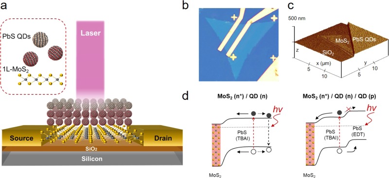
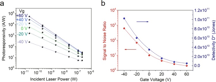
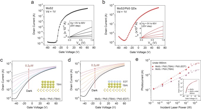
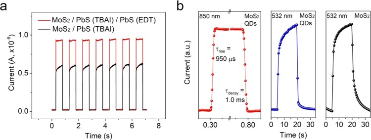
Phototransistors that are based on a hybrid vertical heterojunction structure of two-dimensional (2D)/quantum dots (QDs) have recently attracted attention as a promising device architecture for enhancing the quantum efficiency of photodetectors. However, to optimize the device structure to allow for more efficient charge separation and transfer to the electrodes, a better understanding of the photophysical mechanisms that take place in these architectures is required. Here, we employ a novel concept involving the modulation of the built-in potential within the QD layers for creating a new hybrid MoS/PbS QDs phototransistor with consecutive type II junctions. The effects of the built-in potential across the depletion region near the type II junction interface in the QD layers are found to improve the photoresponse as well as decrease the response times to 950 μs, which is the faster response time (by orders of magnitude) than that recorded for previously reported 2D/QD phototransistors. Also, by implementing an electric-field modulation of the MoS channel, our experimental results reveal that the detectivity can be as large as 1 × 10 jones. This work demonstrates an important pathway toward designing hybrid phototransistors and mixed-dimensional van der Waals heterostructures.
基于二维(2D)/量子点(QD)混合垂直异质结结构的光电晶体管,作为一种提高光电探测器量子效率的有前景的器件架构,近来受到了关注。然而,为了优化器件结构以实现更高效的电荷分离并传输至电极,需要更好地理解这些架构中发生的光物理机制。在此,我们采用了一种新颖的概念,即通过调制量子点层内的内建电势来创建一种具有连续II型结的新型混合MoS/PbS量子点光电晶体管。结果发现,量子点层中II型结界面附近耗尽区的内建电势效应可改善光响应,并将响应时间缩短至950微秒,这是比先前报道的2D/量子点光电晶体管记录的响应时间(快几个数量级)更快的响应时间。此外,通过对MoS沟道实施电场调制,我们的实验结果表明探测率可达1×10琼斯。这项工作展示了设计混合光电晶体管和混合维度范德华异质结构的一条重要途径。