De Teresa José María, Orús Pablo, Córdoba Rosa, Philipp Patrick
Instituto de Ciencia de Materiales de Aragón (ICMA, CSIC-Universidad de Zaragoza) and Departamento de Física de la Materia Condensada, Facultad de Ciencias, Universidad de Zaragoza, Calle Pedro Cerbuna 12, 50009 Zaragoza, Spain.
Laboratorio de Microscopías Avanzadas (LMA), Instituto de Nanociencia de Aragón (INA), Edificio de I+D, Campus Río Ebro, 50018 Zaragoza, Spain.
Micromachines (Basel). 2019 Nov 21;10(12):799. doi: 10.3390/mi10120799.
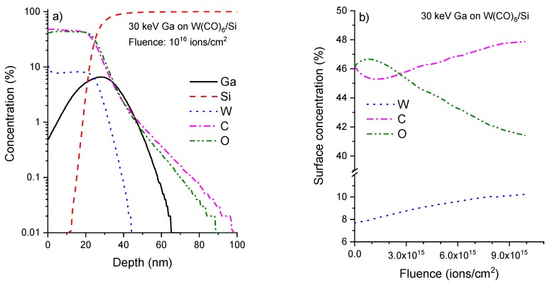
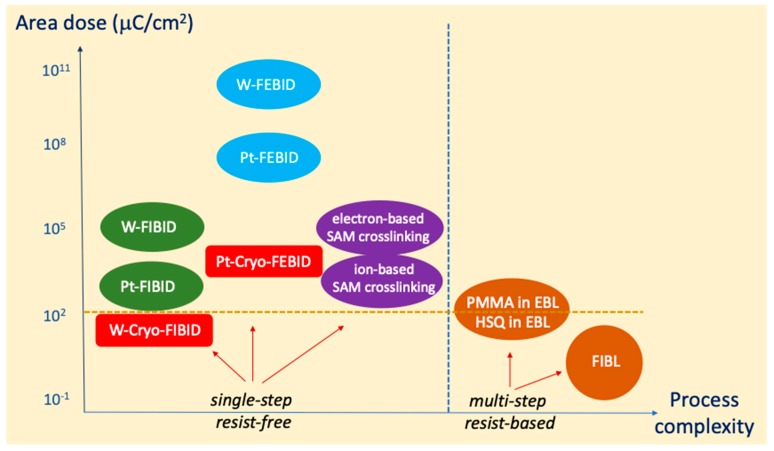
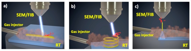
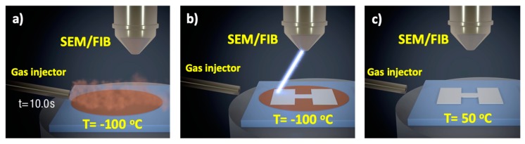
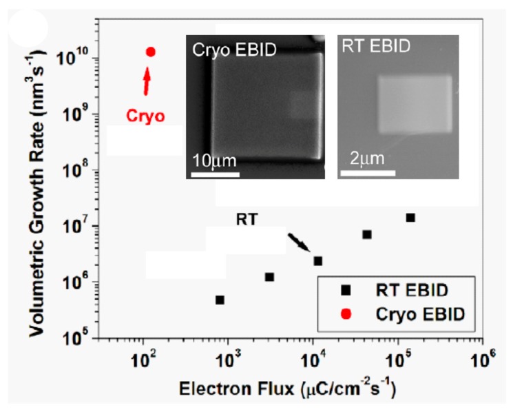
In this contribution, we compare the performance of Focused Electron Beam-induced Deposition (FEBID) and Focused Ion Beam-induced Deposition (FIBID) at room temperature and under cryogenic conditions (the prefix "Cryo" is used here for cryogenic). Under cryogenic conditions, the precursor material condensates on the substrate, forming a layer that is several nm thick. Its subsequent exposure to a focused electron or ion beam and posterior heating to 50 °C reveals the deposit. Due to the extremely low charge dose required, Cryo-FEBID and Cryo-FIBID are found to excel in terms of growth rate, which is typically a few hundred/thousand times higher than room-temperature deposition. Cryo-FIBID using the W(CO) precursor has demonstrated the growth of metallic deposits, with resistivity not far from the corresponding deposits grown at room temperature. This paves the way for its application in circuit edit and the fast and direct growth of micro/nano-electrical contacts with decreased ion damage. The last part of the contribution is dedicated to the comparison of these techniques with other charge-based lithography techniques in terms of the charge dose required and process complexity. The comparison indicates that Cryo-FIBID is very competitive and shows great potential for future lithography developments.
在本论文中,我们比较了聚焦电子束诱导沉积(FEBID)和聚焦离子束诱导沉积(FIBID)在室温及低温条件下(此处“低温”用前缀“Cryo”表示)的性能。在低温条件下,前驱体材料会在基底上凝结,形成一层几纳米厚的薄膜。随后将其暴露于聚焦电子束或离子束下,并加热至50°C,沉积物便会显现出来。由于所需的电荷剂量极低,发现低温FEBID和低温FIBID在生长速率方面表现出色,其生长速率通常比室温沉积高出几百/几千倍。使用W(CO)前驱体的低温FIBID已证明能够生长出金属沉积物,其电阻率与室温下生长的相应沉积物相差不大。这为其在电路编辑以及减少离子损伤的微/纳电接触快速直接生长中的应用铺平了道路。论文的最后一部分致力于在所需电荷剂量和工艺复杂性方面将这些技术与其他基于电荷的光刻技术进行比较。比较结果表明,低温FIBID具有很强的竞争力,在未来光刻技术发展中显示出巨大潜力。