Nambiar Siddharth, Ranganath Praveen, Kallega Rakshitha, Selvaraja Shankar Kumar
Center for Nanoscience and Engineering, Indian Institute of Science, Bengaluru, 560012, India.
Sci Rep. 2019 Dec 11;9(1):18821. doi: 10.1038/s41598-019-55140-8.
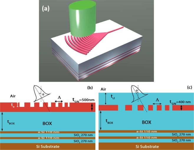
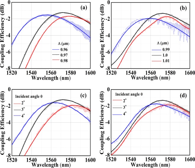
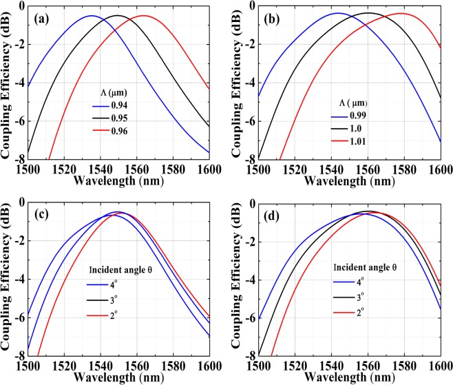
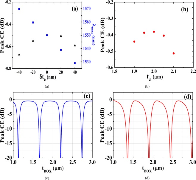
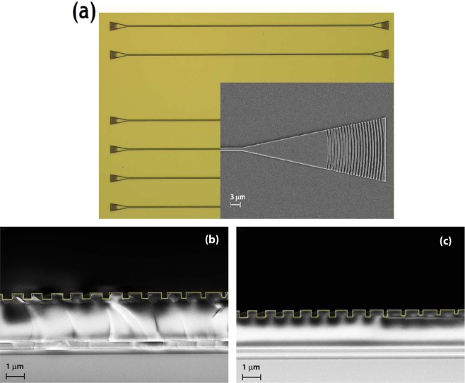
Silicon Nitride (SiN) is emerging as a promising material for a variety of integrated photonic applications. Given its low index contrast however, a key challenge remains to design efficient couplers for the numerous platforms in SiN photonics portfolio. Using a combination of bottom reflector and a chirp generating algorithm, we propose and demonstrate high efficiency, grating couplers on two distinct SiN platforms. For a partially etched grating on 500 nm thick SiN, a calculated peak efficiency of -0.5 dB/coupler is predicted, while for a fully etched grating on 400 nm thick SiN, an efficiency of -0.4 dB/coupler is predicted. Experimentally measured coupling efficiencies are observed to be -1.17 and -1.24 dB/coupler for the partial and fully etched grating couplers respectively in the C-L band region. Furthermore, through numerical simulations, it is shown that the chirping algorithm can be implemented in eight additional combinations comprising SiN film thickness between 300-700 nm as well as alternate claddings, to achieve a per coupler loss between -0.33 to -0.65 dB.
氮化硅(SiN)正成为用于各种集成光子应用的一种有前景的材料。然而,鉴于其低折射率对比度,为SiN光子学产品组合中的众多平台设计高效耦合器仍然是一个关键挑战。通过结合底部反射器和啁啾生成算法,我们在两个不同的SiN平台上提出并演示了高效光栅耦合器。对于500nm厚的SiN上的部分蚀刻光栅,预测的计算峰值效率为-0.5dB/耦合器,而对于400nm厚的SiN上的完全蚀刻光栅,预测效率为-0.4dB/耦合器。在C-L波段区域,实验测量的部分蚀刻和完全蚀刻光栅耦合器的耦合效率分别为-1.17和-1.24dB/耦合器。此外,通过数值模拟表明,啁啾算法可以在包括300 - 700nm之间的SiN膜厚度以及交替包层的另外八种组合中实现,以实现每个耦合器-0.33至-0.65dB的损耗。