Williams Calum, Gordon George S D, Wilkinson Timothy D, Bohndiek Sarah E
Electrical Engineering Division, Department of Engineering, University of Cambridge, 9 JJ Thomson Avenue, Cambridge, CB3 0FA, U.K.
Department of Physics, Cavendish Laboratory, University of Cambridge, JJ Thomson Avenue, Cambridge, CB3 0HE, U.K.
ACS Photonics. 2019 Dec 18;6(12):3132-3141. doi: 10.1021/acsphotonics.9b01196. Epub 2019 Oct 23.
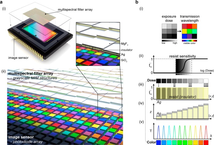
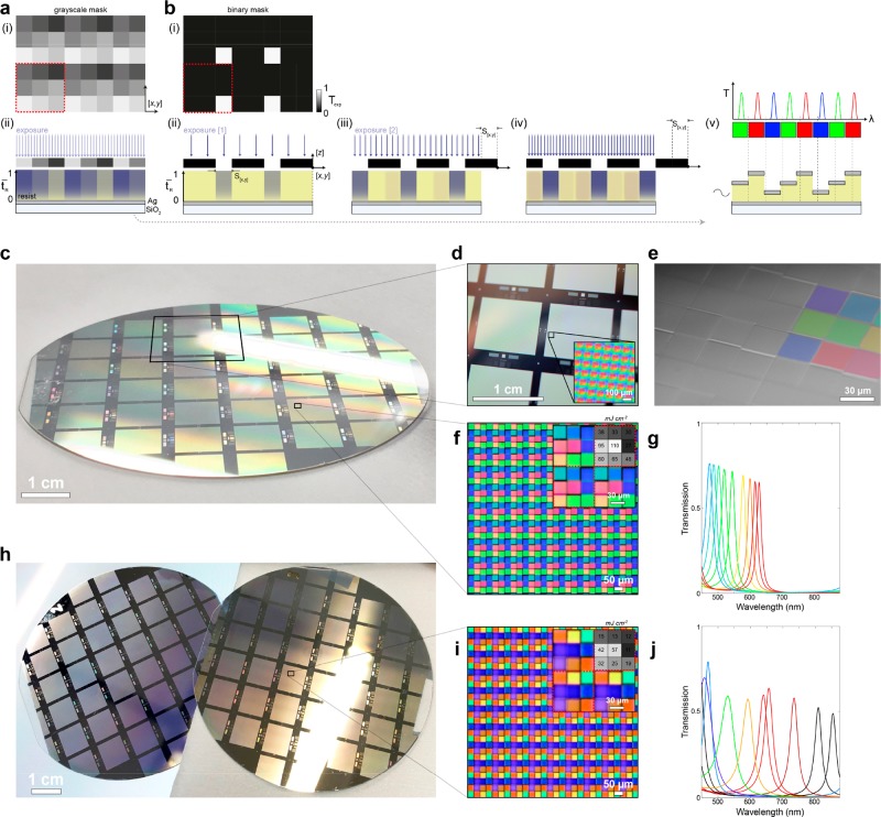
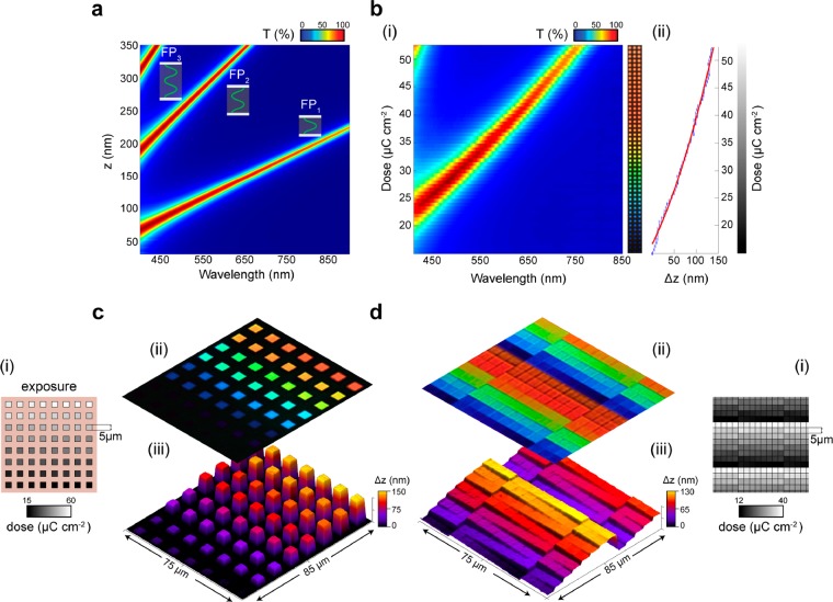
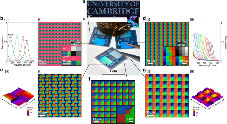
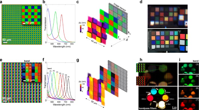
Snapshot multispectral image (MSI) sensors have been proposed as a key enabler for a plethora of multispectral imaging applications, from diagnostic medical imaging to remote sensing. With each application requiring a different set, and number, of spectral bands, the absence of a scalable, cost-effective manufacturing solution for custom multispectral filter arrays (MSFAs) has prevented widespread MSI adoption. Despite recent nanophotonic-based efforts, such as plasmonic or high-index metasurface arrays, large-area MSFA manufacturing still consists of many-layer dielectric (Fabry-Perot) stacks, requiring separate complex lithography steps for each spectral band and multiple material compositions for each. It is an expensive, cumbersome, and inflexible undertaking, but yields optimal optical performance. Here, we demonstrate a manufacturing process that enables cost-effective wafer-level fabrication of custom MSFAs in a single lithographic step, maintaining high efficiencies (∼75%) and narrow line widths (∼25 nm) across the visible to near-infrared. By merging grayscale (analog) lithography with metal-insulator-metal (MIM) Fabry-Perot cavities, whereby exposure dose controls cavity thickness, we demonstrate simplified fabrication of MSFAs up to -wavelength bands. The concept is first proven using low-volume electron beam lithography, followed by the demonstration of large-volume UV mask-based photolithography with MSFAs produced at the wafer level. Our framework provides an attractive alternative to conventional MSFA manufacture and metasurface-based spectral filters by reducing both fabrication complexity and cost of these intricate optical devices, while increasing customizability.
快照多光谱图像(MSI)传感器已被视为众多多光谱成像应用的关键推动因素,涵盖从诊断医学成像到遥感等领域。由于每种应用都需要不同的光谱带集合和数量,缺乏用于定制多光谱滤光片阵列(MSFA)的可扩展、经济高效的制造解决方案阻碍了MSI的广泛应用。尽管最近有基于纳米光子学的努力,如等离子体或高折射率超表面阵列,但大面积MSFA制造仍然由多层电介质(法布里 - 珀罗)堆叠组成,每个光谱带都需要单独的复杂光刻步骤,并且每个步骤都需要多种材料成分。这是一项昂贵、繁琐且不灵活的工作,但能产生最佳的光学性能。在这里,我们展示了一种制造工艺,该工艺能够在单个光刻步骤中以具有成本效益的方式在晶圆级制造定制的MSFA,在可见光到近红外范围内保持高效率(约75%)和窄线宽(约25纳米)。通过将灰度(模拟)光刻与金属 - 绝缘体 - 金属(MIM)法布里 - 珀罗腔相结合,曝光剂量可控制腔厚度,我们展示了高达 - 波长波段的MSFA的简化制造。该概念首先通过低产量电子束光刻得到验证,随后展示了基于紫外掩膜的大批量光刻,并在晶圆级生产了MSFA。我们的框架通过降低这些复杂光学器件的制造复杂性和成本,同时提高可定制性,为传统MSFA制造和基于超表面的光谱滤光片提供了一种有吸引力的替代方案。