Oksenberg Eitan, Merdasa Aboma, Houben Lothar, Kaplan-Ashiri Ifat, Rothman Amnon, Scheblykin Ivan G, Unger Eva L, Joselevich Ernesto
Department of Materials and Interfaces Weizmann Institute of Science, Rehovot, 76100, Israel.
Helmholtz-Zentrum Berlin GmbH, Young Investigator Group Hybrid Materials Formation and Scaling, Albert Einstein Straße 16, Berlin, 12489, Germany.
Nat Commun. 2020 Jan 24;11(1):489. doi: 10.1038/s41467-020-14365-2.
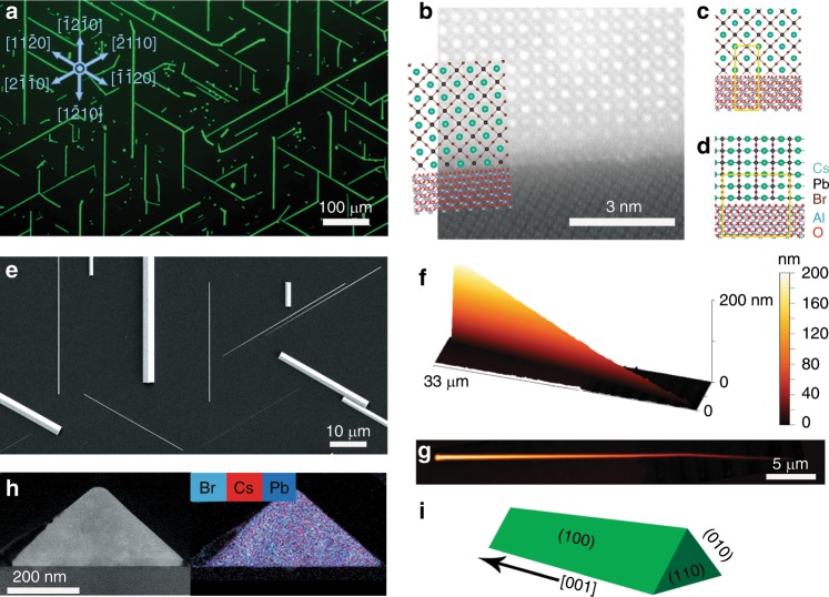
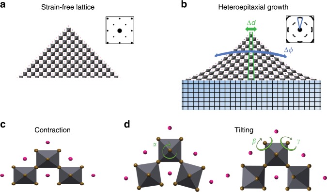
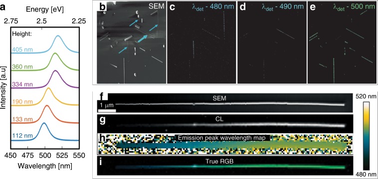
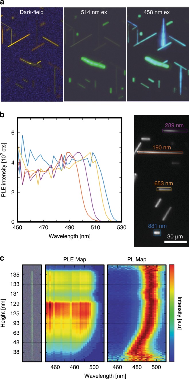
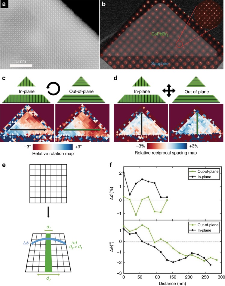
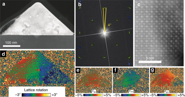
Metal-halide perovskites have been shown to be remarkable and promising optoelectronic materials. However, despite ongoing research from multiple perspectives, some fundamental questions regarding their optoelectronic properties remain controversial. One reason is the high-variance of data collected from, often unstable, polycrystalline thin films. Here we use ordered arrays of stable, single-crystal cesium lead bromide (CsPbBr) nanowires grown by surface-guided chemical vapor deposition to study fundamental properties of these semiconductors in a one-dimensional model system. Specifically, we uncover the origin of an unusually large size-dependent luminescence emission spectral blue-shift. Using multiple spatially resolved spectroscopy techniques, we establish that bandgap modulation causes the emission shift, and by correlation with state-of-the-art electron microscopy methods, we reveal its origin in substantial and uniform lattice rotations due to heteroepitaxial strain and lattice relaxation. Understanding strain and its effect on the optoelectronic properties of these dynamic materials, from the atomic scale up, is essential to evaluate their performance limits and fundamentals of charge carrier dynamics.
金属卤化物钙钛矿已被证明是卓越且有前景的光电子材料。然而,尽管从多个角度进行了持续研究,但关于其光电子性质的一些基本问题仍存在争议。一个原因是从通常不稳定的多晶薄膜收集的数据具有高方差性。在此,我们使用通过表面引导化学气相沉积生长的稳定的单晶溴化铯铅(CsPbBr)纳米线的有序阵列,在一维模型系统中研究这些半导体的基本性质。具体而言,我们揭示了异常大的尺寸依赖性发光发射光谱蓝移的起源。使用多种空间分辨光谱技术,我们确定带隙调制导致发射位移,并且通过与最先进的电子显微镜方法相关联,我们揭示其起源于由于异质外延应变和晶格弛豫导致的大量且均匀的晶格旋转。从原子尺度开始理解应变及其对这些动态材料光电子性质的影响,对于评估其性能极限和电荷载流子动力学的基本原理至关重要。