Bioelectronics (IBI-3), Forschungszentrum Jülich, 52425, Jülich, Germany.
LIMMS-CNRS/IIS, Institute of Industrial Science, The University of Tokyo, Tokyo, 153-8505, Japan.
Sci Rep. 2020 Jul 29;10(1):12678. doi: 10.1038/s41598-020-69493-y.
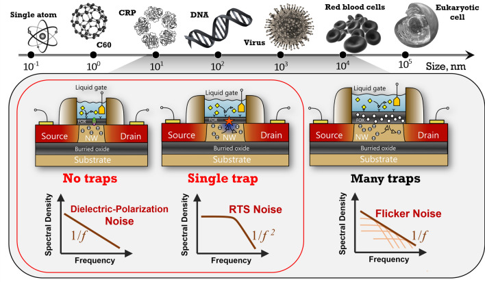
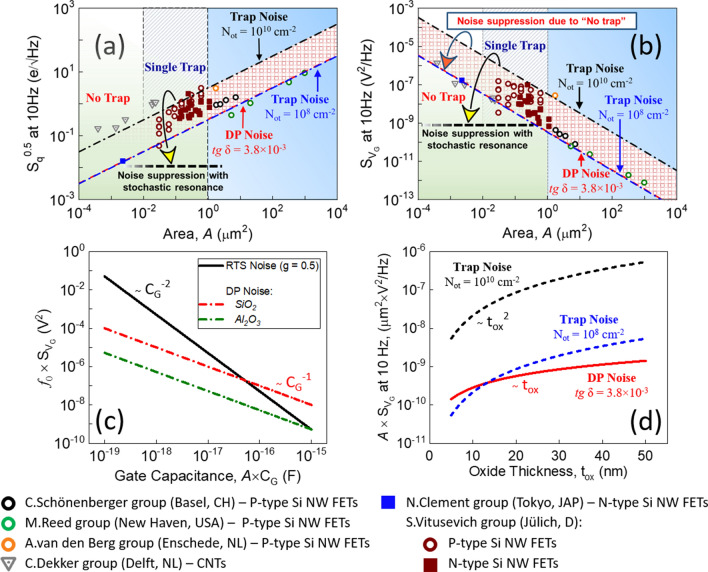
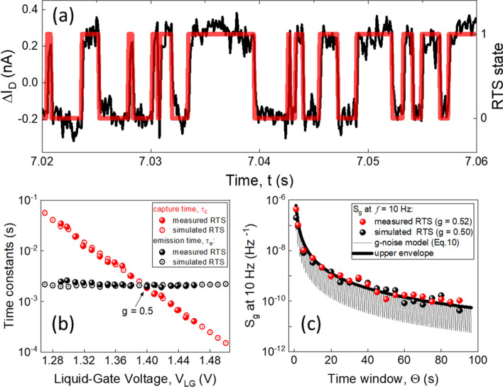
Transistor biosensors are mass-fabrication-compatible devices of interest for point of care diagnosis as well as molecular interaction studies. While the actual transistor gates in processors reach the sub-10 nm range for optimum integration and power consumption, studies on design rules for the signal-to-noise ratio (S/N) optimization in transistor-based biosensors have been so far restricted to 1 µm device gate area, a range where the discrete nature of the defects can be neglected. In this study, which combines experiments and theoretical analysis at both numerical and analytical levels, we extend such investigation to the nanometer range and highlight the effect of doping type as well as the noise suppression opportunities offered at this scale. In particular, we show that, when a single trap is active near the conductive channel, the noise can be suppressed even beyond the thermal limit by monitoring the trap occupancy probability in an approach analog to the stochastic resonance effect used in biological systems.
晶体管生物传感器是大规模制造兼容的设备,适用于即时诊断和分子相互作用研究。虽然处理器中的实际晶体管栅极达到亚 10nm 的范围以实现最佳集成和功耗,但迄今为止,关于基于晶体管的生物传感器中信号噪声比 (S/N) 优化的设计规则的研究仅限于 1µm 的器件栅极面积,在该范围内可以忽略缺陷的离散性质。在这项研究中,我们结合了数值和分析水平的实验和理论分析,将这种研究扩展到纳米范围,并强调了掺杂类型的影响以及在该尺度下提供的噪声抑制机会。特别是,我们表明,当单个陷阱在导电通道附近活跃时,通过监测陷阱占据概率,可以抑制噪声,甚至超越热极限,这种方法类似于生物系统中使用的随机共振效应。