Alhalaili Badriyah, Bunk Ryan James, Mao Howard, Cansizoglu Hilal, Vidu Ruxandra, Woodall Jerry, Islam M Saif
Nanotechnology and Advanced Materials Program, Kuwait Institute for Scientific Research, Kuwait City, Kuwait.
Department of Electrical and Computer Engineering, University of California, Davis, Davis, USA.
Sci Rep. 2020 Dec 8;10(1):21434. doi: 10.1038/s41598-020-78326-x.
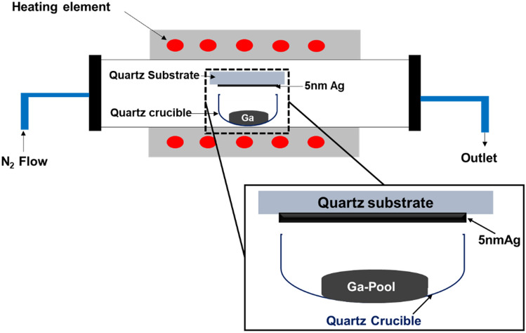
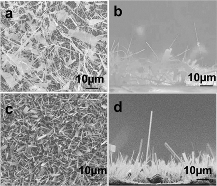
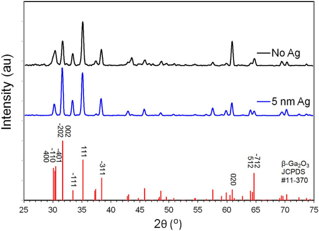
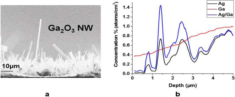
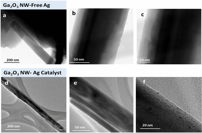
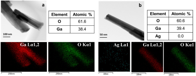
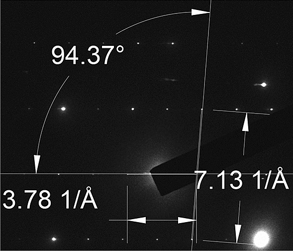
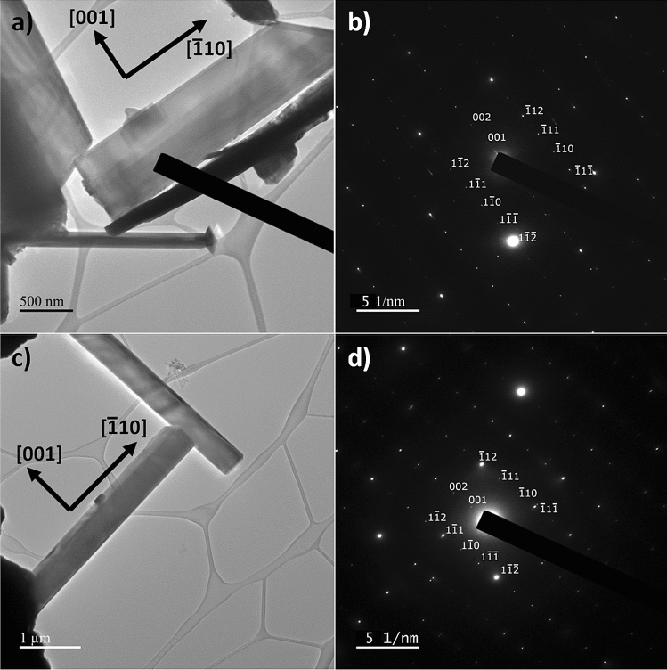
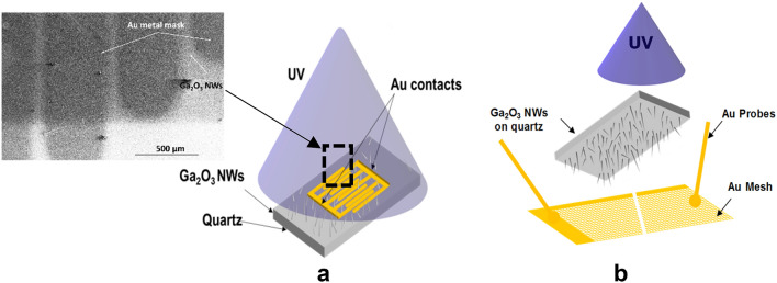
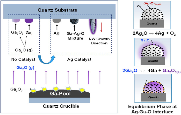
In the last decade, interest in the use of beta gallium oxide (β-GaO) as a semiconductor for high power/high temperature devices and deep-UV sensors has grown. GaO has an enormous band gap of 4.8 eV, which makes it well suited for these applications. Compared to thin films, nanowires exhibit a higher surface-to-volume ratio, increasing their sensitivity for detection of chemical substances and light. In this work, we explore a simple and inexpensive method of growing high-density gallium oxide nanowires at high temperatures. Gallium oxide nanowire growth can be achieved by heating and oxidizing pure gallium at high temperatures (~ 1000 °C) in the presence of trace amounts of oxygen. This process can be optimized to large-scale production to grow high-quality, dense and long GaO nanowires. We show the results of morphological, structural, electrical and optical characterization of the β-GaO nanowires including the optical bandgap and photoconductance. The influence of density on these GaO nanowires and their properties will be examined in order to determine the optimum configuration for the detection of UV light.
在过去十年中,人们对将β-氧化镓(β-GaO)用作高功率/高温器件及深紫外传感器的半导体的兴趣与日俱增。氧化镓具有4.8电子伏特的巨大带隙,这使其非常适合这些应用。与薄膜相比,纳米线具有更高的表面积与体积比,从而提高了它们对化学物质和光的检测灵敏度。在这项工作中,我们探索了一种在高温下生长高密度氧化镓纳米线的简单且低成本的方法。通过在微量氧气存在下于高温(约1000°C)加热并氧化纯镓,可实现氧化镓纳米线的生长。此过程可优化用于大规模生产,以生长高质量、高密度且长的氧化镓纳米线。我们展示了β-GaO纳米线的形态、结构、电学和光学特性表征结果,包括光学带隙和光电导。为了确定用于紫外光检测的最佳配置,将研究密度对这些氧化镓纳米线及其性能的影响。