Gnatyuk Volodymyr, Maslyanchuk Olena, Solovan Mykhailo, Brus Viktor, Aoki Toru
V.E. Lashkaryov Institute of Semiconductor Physics of the National Academy of Sciences of Ukraine, Prospekt Nauky 41, 03028 Kyiv, Ukraine.
Institute of Applied Physics and Computer Sciences, Yuriy Fedkovych Chernivtsi National University, Kotsyubynskyi Str. 2, 58012 Chernivtsi, Ukraine.
Sensors (Basel). 2021 May 18;21(10):3518. doi: 10.3390/s21103518.
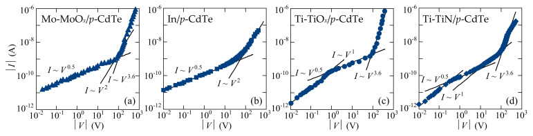
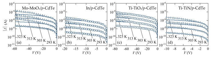
Different contact materials and optimization of techniques of their depositions expand the possibilities to obtain high performance room temperature CdTe-based X/γ-ray detectors. The heterostructures with ohmic (MoO) and Schottky (MoO, TiO, TiN, and In) contacts, created by DC reactive magnetron sputtering and vacuum thermal evaporation, as well as In/CdTe/Au diodes with a junction, formed by laser-induced doping, have been developed and investigated. Depending on the surface pre-treatment of semi-insulating -CdTe crystals, the deposition of a MoO film formed either ohmic or Schottky contacts. Based on the calculations and characteristics of the Mo-MoO/-CdTe/MoO-Mo, In/-CdTe/MoO-Mo, Ti-TiO/-CdTe/MoO-Mo, and Ti-TiN/-CdTe/MoO-Mo Schottky-diode detectors, the current transport processes were described in the models of the carrier generation-recombination within the space-charge region (SCR) at low bias, and space-charge limited current incorporating the Poole-Frenkel effect at higher voltages, respectively. The energies of generation-recombination centers, density of trapping centers, and effective carrier lifetimes were determined. Nanosecond laser irradiation of the In electrode, pre-deposited on the -CdTe crystals, resulted in extending the voltage range, corresponding to the carrier generation-recombination in the SCR in the characteristics of the In/CdTe/Au diodes. Such In/CdTe/Au junction diode detectors demonstrated high energy resolutions (7%@59.5 keV, 4%@122 keV, and 1.6%@662 keV).
不同的接触材料及其沉积技术的优化拓展了获得高性能室温碲化镉基X/γ射线探测器的可能性。通过直流反应磁控溅射和真空热蒸发制备了具有欧姆(MoO)和肖特基(MoO、TiO、TiN和In)接触的异质结构,以及通过激光诱导掺杂形成的具有结的In/CdTe/Au二极管,并对其进行了研究。根据半绝缘碲化镉晶体的表面预处理情况,MoO薄膜的沉积形成了欧姆接触或肖特基接触。基于对Mo-MoO/碲化镉/MoO-Mo、In/碲化镉/MoO-Mo、Ti-TiO/碲化镉/MoO-Mo和Ti-TiN/碲化镉/MoO-Mo肖特基二极管探测器的计算和特性,分别在低偏压下的空间电荷区(SCR)内载流子产生-复合模型以及高电压下包含普尔-弗伦克尔效应的空间电荷限制电流模型中描述了电流传输过程。确定了产生-复合中心的能量、俘获中心的密度和有效载流子寿命。对预先沉积在碲化镉晶体上的In电极进行纳秒激光照射,使得In/CdTe/Au二极管特性中对应于SCR内载流子产生-复合的电压范围得以扩展。这种In/CdTe/Au结型二极管探测器展现出了高能量分辨率(在59.5 keV时为7%,在122 keV时为4%,在662 keV时为1.6%)。