Gulka Michal, Wirtitsch Daniel, Ivády Viktor, Vodnik Jelle, Hruby Jaroslav, Magchiels Goele, Bourgeois Emilie, Gali Adam, Trupke Michael, Nesladek Milos
Institute for Materials Research (IMO), Hasselt University, Diepenbeek, Belgium.
Faculty of Biomedical Engineering, Czech Technical University in Prague, Kladno, Czechia.
Nat Commun. 2021 Jul 20;12(1):4421. doi: 10.1038/s41467-021-24494-x.
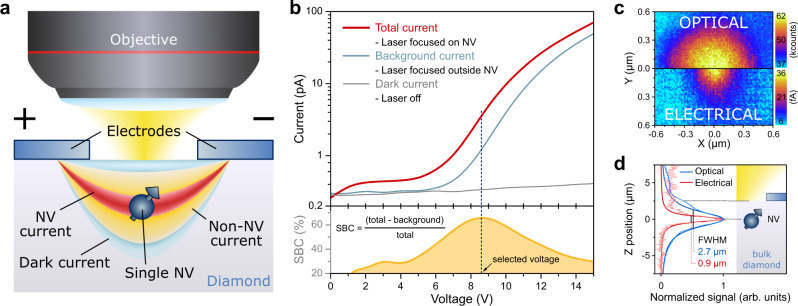
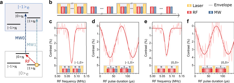
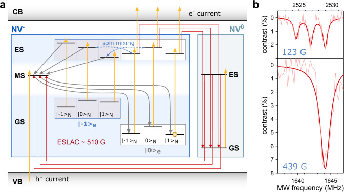
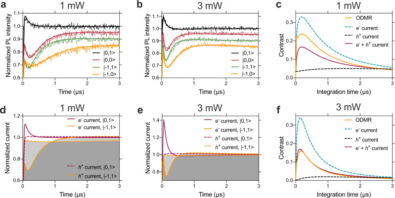
Nuclear spins in semiconductors are leading candidates for future quantum technologies, including quantum computation, communication, and sensing. Nuclear spins in diamond are particularly attractive due to their long coherence time. With the nitrogen-vacancy (NV) centre, such nuclear qubits benefit from an auxiliary electronic qubit, which, at cryogenic temperatures, enables probabilistic entanglement mediated optically by photonic links. Here, we demonstrate a concept of a microelectronic quantum device at ambient conditions using diamond as wide bandgap semiconductor. The basic quantum processor unit - a single N nuclear spin coupled to the NV electron - is read photoelectrically and thus operates in a manner compatible with nanoscale electronics. The underlying theory provides the key ingredients for photoelectric quantum gate operations and readout of nuclear qubit registers. This demonstration is, therefore, a step towards diamond quantum devices with a readout area limited by inter-electrode distance rather than by the diffraction limit. Such scalability could enable the development of electronic quantum processors based on the dipolar interaction of spin-qubits placed at nanoscopic proximity.
半导体中的核自旋是未来量子技术(包括量子计算、通信和传感)的主要候选对象。由于其长相干时间,金刚石中的核自旋特别具有吸引力。借助氮空位(NV)中心,此类核量子比特受益于一个辅助电子量子比特,在低温下,该辅助电子量子比特能通过光子链路实现光学介导的概率纠缠。在此,我们展示了一种在环境条件下使用金刚石作为宽带隙半导体的微电子量子器件概念。基本量子处理器单元——一个与NV电子耦合的单个N核自旋——通过光电方式读取,因此其运行方式与纳米级电子器件兼容。基础理论为光电量子门操作和核量子比特寄存器的读出提供了关键要素。因此,这一演示朝着读出面积受电极间距而非衍射极限限制的金刚石量子器件迈出了一步。这种可扩展性能够推动基于纳米尺度近距离放置的自旋量子比特的偶极相互作用的电子量子处理器的发展。