• 文献检索
  • 文档翻译
  • 深度研究
  • 学术资讯
  • Suppr Zotero 插件Zotero 插件
  • 邀请有礼
  • 套餐&价格
  • 历史记录
应用&插件
Suppr Zotero 插件Zotero 插件浏览器插件Mac 客户端Windows 客户端微信小程序
定价
高级版会员购买积分包购买API积分包
服务
文献检索文档翻译深度研究API 文档MCP 服务
关于我们
关于 Suppr公司介绍联系我们用户协议隐私条款
关注我们

Suppr 超能文献

核心技术专利:CN118964589B侵权必究
粤ICP备2023148730 号-1Suppr @ 2026

文献检索

告别复杂PubMed语法,用中文像聊天一样搜索,搜遍4000万医学文献。AI智能推荐,让科研检索更轻松。

立即免费搜索

文件翻译

保留排版,准确专业,支持PDF/Word/PPT等文件格式,支持 12+语言互译。

免费翻译文档

深度研究

AI帮你快速写综述,25分钟生成高质量综述,智能提取关键信息,辅助科研写作。

立即免费体验

通过结合干涉光刻和灰度图案二次曝光对纳米图案尺寸进行空间调制。

Spatial modulation of nanopattern dimensions by combining interference lithography and grayscale-patterned secondary exposure.

作者信息

Gan Zhuofei, Feng Hongtao, Chen Liyang, Min Siyi, Liang Chuwei, Xu Menghong, Jiang Zijie, Sun Zhao, Sun Chuying, Cui Dehu, Li Wen-Di

机构信息

Department of Mechanical Engineering, University of Hong Kong, Hong Kong, China.

School of Microelectronics, Southern University of Science and Technology, Shenzhen, China.

出版信息

Light Sci Appl. 2022 Apr 8;11(1):89. doi: 10.1038/s41377-022-00774-z.

DOI:10.1038/s41377-022-00774-z
PMID:35396549
原文链接:https://pmc.ncbi.nlm.nih.gov/articles/PMC8993805/
Abstract

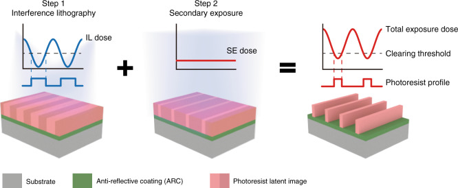
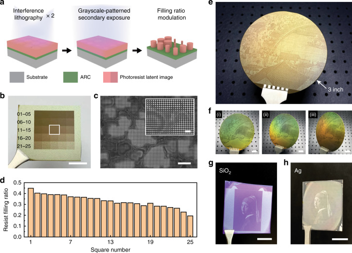
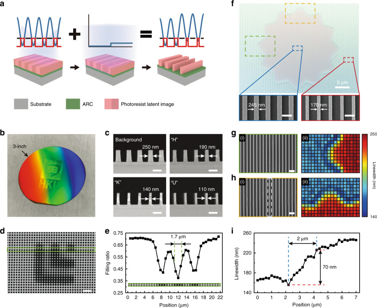
Functional nanostructures are exploited for a variety of cutting-edge fields including plasmonics, metasurfaces, and biosensors, just to name a few. Some applications require nanostructures with uniform feature sizes while others rely on spatially varying morphologies. However, fine manipulation of the feature size over a large area remains a substantial challenge because mainstream approaches to precise nanopatterning are based on low-throughput pixel-by-pixel processing, such as those utilizing focused beams of photons, electrons, or ions. In this work, we provide a solution toward wafer-scale, arbitrary modulation of feature size distribution by introducing a lithographic portfolio combining interference lithography (IL) and grayscale-patterned secondary exposure (SE). Employed after the high-throughput IL, a SE with patterned intensity distribution spatially modulates the dimensions of photoresist nanostructures. Based on this approach, we successfully fabricated 4-inch wafer-scale nanogratings with uniform linewidths of <5% variation, using grayscale-patterned SE to compensate for the linewidth difference caused by the Gaussian distribution of the laser beams in the IL. Besides, we also demonstrated a wafer-scale structural color painting by spatially modulating the filling ratio to achieve gradient grayscale color using SE.

摘要

功能纳米结构被应用于包括等离激元学、超表面和生物传感器等在内的各种前沿领域,仅举几例。一些应用需要具有均匀特征尺寸的纳米结构,而其他一些则依赖于空间变化的形态。然而,在大面积上精细控制特征尺寸仍然是一个重大挑战,因为精确纳米图案化的主流方法是基于低通量的逐像素处理,例如那些利用光子、电子或离子聚焦束的方法。在这项工作中,我们通过引入一种结合干涉光刻(IL)和灰度图案二次曝光(SE)的光刻组合,提供了一种实现晶圆级特征尺寸分布任意调制的解决方案。在高通量IL之后使用,具有图案化强度分布的SE在空间上调制光刻胶纳米结构的尺寸。基于这种方法,我们成功制造了4英寸晶圆级纳米光栅,其均匀线宽变化小于5%,使用灰度图案化SE来补偿IL中激光束高斯分布引起的线宽差异。此外,我们还通过使用SE空间调制填充率以实现梯度灰度颜色,展示了晶圆级结构彩色图案。

https://cdn.ncbi.nlm.nih.gov/pmc/blobs/df8a/8993805/66f444992945/41377_2022_774_Fig5_HTML.jpg
https://cdn.ncbi.nlm.nih.gov/pmc/blobs/df8a/8993805/e2f9179b9d04/41377_2022_774_Fig1_HTML.jpg
https://cdn.ncbi.nlm.nih.gov/pmc/blobs/df8a/8993805/3e0a1ad53a7b/41377_2022_774_Fig2_HTML.jpg
https://cdn.ncbi.nlm.nih.gov/pmc/blobs/df8a/8993805/18b0cb97ec90/41377_2022_774_Fig3_HTML.jpg
https://cdn.ncbi.nlm.nih.gov/pmc/blobs/df8a/8993805/417daa2c4f63/41377_2022_774_Fig4_HTML.jpg
https://cdn.ncbi.nlm.nih.gov/pmc/blobs/df8a/8993805/66f444992945/41377_2022_774_Fig5_HTML.jpg

相似文献

1
Spatial modulation of nanopattern dimensions by combining interference lithography and grayscale-patterned secondary exposure.通过结合干涉光刻和灰度图案二次曝光对纳米图案尺寸进行空间调制。
Light Sci Appl. 2022 Apr 8;11(1):89. doi: 10.1038/s41377-022-00774-z.
2
Spatial modulation of scalable nanostructures by combining maskless plasmonic lithography and grayscale-patterned strategy.通过结合无掩膜等离子体光刻和灰度图案化策略对可扩展纳米结构进行空间调制。
Nanoscale Adv. 2023 Jun 26;5(17):4424-4434. doi: 10.1039/d3na00147d. eCollection 2023 Aug 24.
3
Gradient wettability induced by deterministically patterned nanostructures.由确定性图案化纳米结构诱导的梯度润湿性。
Microsyst Nanoeng. 2020 Nov 30;6:106. doi: 10.1038/s41378-020-00215-0. eCollection 2020.
4
Nanostructures and functional materials fabricated by interferometric lithography.利用干涉光刻技术制造的纳米结构和功能材料。
Adv Mater. 2011 Jan 11;23(2):147-79. doi: 10.1002/adma.201001856.
5
Combining thermal scanning probe lithography and dry etching for grayscale nanopattern amplification.结合热扫描探针光刻和干法蚀刻实现灰度纳米图案放大。
Microsyst Nanoeng. 2024 Feb 23;10:28. doi: 10.1038/s41378-024-00655-y. eCollection 2024.
6
Nanopatterning by laser interference lithography: applications to optical devices.基于激光干涉光刻的纳米图案化技术:在光学器件中的应用
J Nanosci Nanotechnol. 2014 Feb;14(2):1521-32. doi: 10.1166/jnn.2014.9199.
7
Sub-wavelength patterned pulse laser lithography for efficient fabrication of large-area metasurfaces.用于高效制造大面积超表面的亚波长图案化脉冲激光光刻技术。
Nat Commun. 2022 Oct 3;13(1):5823. doi: 10.1038/s41467-022-33644-8.
8
Large-area pattern transfer of metallic nanostructures on glass substrates via interference lithography.通过干涉光刻在玻璃衬底上实现大面积金属纳米结构的图案转移。
Nanotechnology. 2011 Jul 15;22(28):285306. doi: 10.1088/0957-4484/22/28/285306. Epub 2011 Jun 6.
9
Massively parallel direct writing of nanoapertures using multi-optical probes and super-resolution near-fields.使用多光学探针和超分辨率近场进行纳米孔径的大规模并行直接写入。
Microsyst Nanoeng. 2022 Sep 15;8:101. doi: 10.1038/s41378-022-00416-9. eCollection 2022.
10
Full Color and Grayscale Painting with 3D Printed Low-Index Nanopillars.采用3D打印低折射率纳米柱的全彩和灰度绘画
Nano Lett. 2021 Jun 9;21(11):4721-4729. doi: 10.1021/acs.nanolett.1c00979. Epub 2021 May 21.

引用本文的文献

1
Advancements and challenges in inverse lithography technology: a review of artificial intelligence-based approaches.逆光刻技术的进展与挑战:基于人工智能方法的综述
Light Sci Appl. 2025 Jul 24;14(1):250. doi: 10.1038/s41377-025-01923-w.
2
Controlling the wavefront aberration of a large-aperture and high-precision holographic diffraction grating.控制大口径高精度全息衍射光栅的波前像差。
Light Sci Appl. 2025 Mar 5;14(1):112. doi: 10.1038/s41377-025-01785-2.
3
Generic characterization method for nano-gratings using deep-neural-network-assisted ellipsometry.

本文引用的文献

1
Reconfiguring Colors of Single Relief Structures by Directional Stretching.通过定向拉伸重新配置单一浮雕结构的颜色。
Adv Mater. 2022 Feb;34(6):e2108128. doi: 10.1002/adma.202108128. Epub 2021 Dec 26.
2
Gradient wettability induced by deterministically patterned nanostructures.由确定性图案化纳米结构诱导的梯度润湿性。
Microsyst Nanoeng. 2020 Nov 30;6:106. doi: 10.1038/s41378-020-00215-0. eCollection 2020.
3
Ultrasensitive Molecular Detection by Imaging of Centimeter-Scale Metasurfaces with a Deterministic Gradient Geometry.
基于深度神经网络辅助椭偏仪的纳米光栅通用表征方法
Nanophotonics. 2024 Jan 16;13(7):1181-1189. doi: 10.1515/nanoph-2023-0798. eCollection 2024 Mar.
4
Objective-Free Ultrasensitive Biosensing on Large-Area Metamaterial Surfaces in the Near-IR.近红外光下大面积超材料表面无标记超灵敏生物传感
ACS Appl Mater Interfaces. 2024 Jun 26;16(25):32516-32523. doi: 10.1021/acsami.4c04777. Epub 2024 Jun 13.
5
Spatial modulation of scalable nanostructures by combining maskless plasmonic lithography and grayscale-patterned strategy.通过结合无掩膜等离子体光刻和灰度图案化策略对可扩展纳米结构进行空间调制。
Nanoscale Adv. 2023 Jun 26;5(17):4424-4434. doi: 10.1039/d3na00147d. eCollection 2023 Aug 24.
6
Laser Interference Lithography-A Method for the Fabrication of Controlled Periodic Structures.激光干涉光刻——一种制备可控周期结构的方法
Nanomaterials (Basel). 2023 Jun 7;13(12):1818. doi: 10.3390/nano13121818.
利用具有确定性梯度几何形状的厘米级超材料实现超灵敏分子成像检测。
Adv Mater. 2021 Jul;33(29):e2100270. doi: 10.1002/adma.202100270. Epub 2021 Jun 4.
4
Full Color and Grayscale Painting with 3D Printed Low-Index Nanopillars.采用3D打印低折射率纳米柱的全彩和灰度绘画
Nano Lett. 2021 Jun 9;21(11):4721-4729. doi: 10.1021/acs.nanolett.1c00979. Epub 2021 May 21.
5
Functional THz emitters based on Pancharatnam-Berry phase nonlinear metasurfaces.基于潘查拉特纳姆-贝里相位非线性超表面的功能性太赫兹发射器。
Nat Commun. 2021 Jan 4;12(1):30. doi: 10.1038/s41467-020-20283-0.
6
Printable Nanocomposite Metalens for High-Contrast Near-Infrared Imaging.用于高对比度近红外成像的可打印纳米复合超颖透镜
ACS Nano. 2021 Jan 26;15(1):698-706. doi: 10.1021/acsnano.0c06968. Epub 2021 Jan 1.
7
Metasurface-driven OLED displays beyond 10,000 pixels per inch.基于超表面的 OLED 显示器,像素密度超过每英寸 10000 个。
Science. 2020 Oct 23;370(6515):459-463. doi: 10.1126/science.abc8530.
8
Single-step manufacturing of hierarchical dielectric metalens in the visible.可见光波段分层介质超透镜的一步法制造
Nat Commun. 2020 May 8;11(1):2268. doi: 10.1038/s41467-020-16136-5.
9
All-dielectric metasurface for high-performance structural color.用于高性能结构色的全介质超表面
Nat Commun. 2020 Apr 20;11(1):1864. doi: 10.1038/s41467-020-15773-0.
10
Design of a uniform-illumination two-dimensional waveguide head-up display with thin plate compensator.带有薄板补偿器的均匀照明二维波导平视显示器的设计
Opt Express. 2019 Apr 29;27(9):12692-12709. doi: 10.1364/OE.27.012692.