• 文献检索
  • 文档翻译
  • 深度研究
  • 学术资讯
  • Suppr Zotero 插件Zotero 插件
  • 邀请有礼
  • 套餐&价格
  • 历史记录
应用&插件
Suppr Zotero 插件Zotero 插件浏览器插件Mac 客户端Windows 客户端微信小程序
定价
高级版会员购买积分包购买API积分包
服务
文献检索文档翻译深度研究API 文档MCP 服务
关于我们
关于 Suppr公司介绍联系我们用户协议隐私条款
关注我们

Suppr 超能文献

核心技术专利:CN118964589B侵权必究
粤ICP备2023148730 号-1Suppr @ 2026

文献检索

告别复杂PubMed语法,用中文像聊天一样搜索,搜遍4000万医学文献。AI智能推荐,让科研检索更轻松。

立即免费搜索

文件翻译

保留排版,准确专业,支持PDF/Word/PPT等文件格式,支持 12+语言互译。

免费翻译文档

深度研究

AI帮你快速写综述,25分钟生成高质量综述,智能提取关键信息,辅助科研写作。

立即免费体验

在四天内实现平面3D打印微电极阵列的创客空间微制造技术和材料的优化。

Optimization of makerspace microfabrication techniques and materials for the realization of planar, 3D printed microelectrode arrays in under four days.

作者信息

Kundu Avra, Nattoo Crystal, Fremgen Sarah, Springer Sandra, Ausaf Tariq, Rajaraman Swaminathan

机构信息

NanoScience Technology Center (NSTC), University of Central Florida Research I, Office 237, 4353 Scorpius Street Orlando FL 32816-0120 USA

Department of Electrical and Computer Engineering, University of Miami Coral Gables FL 33146 USA.

出版信息

RSC Adv. 2019 Mar 18;9(16):8949-8963. doi: 10.1039/c8ra09116a. eCollection 2019 Mar 15.

DOI:10.1039/c8ra09116a
PMID:35517709
原文链接:https://pmc.ncbi.nlm.nih.gov/articles/PMC9062012/
Abstract

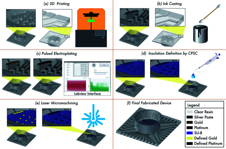
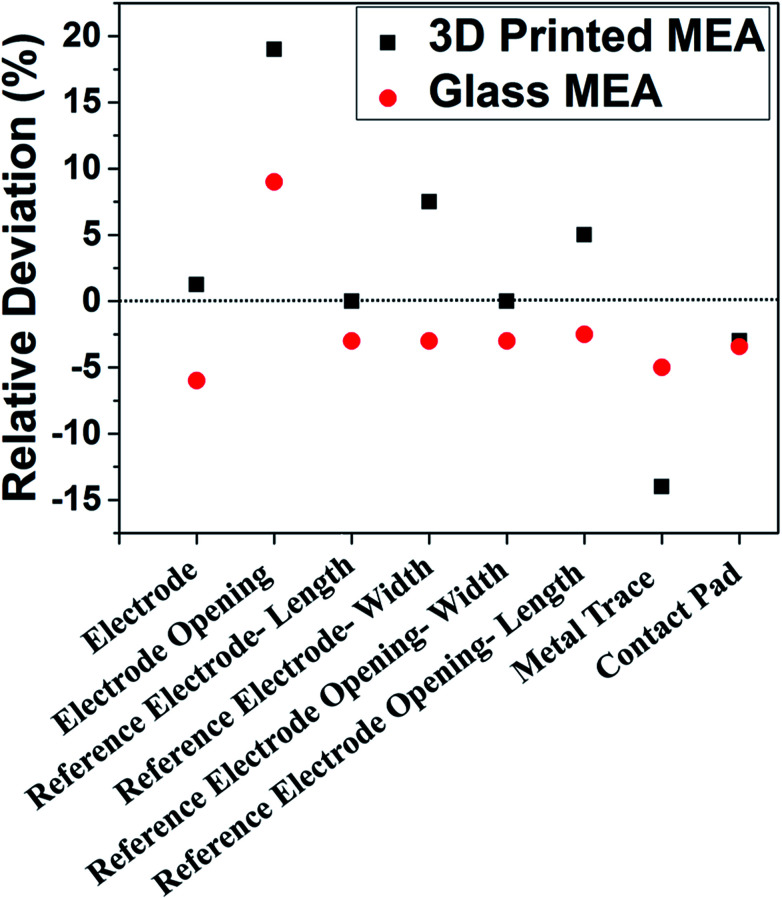
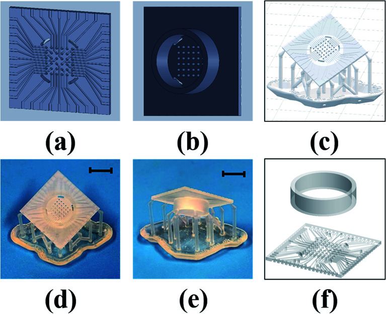
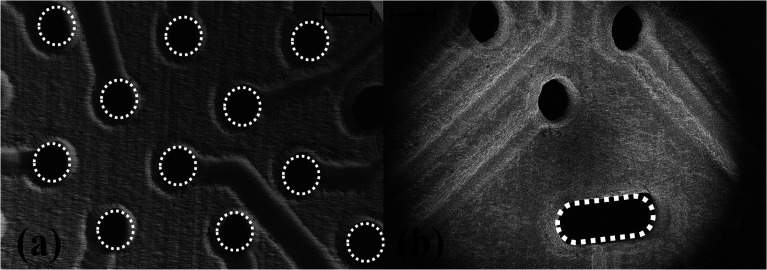
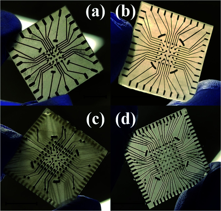
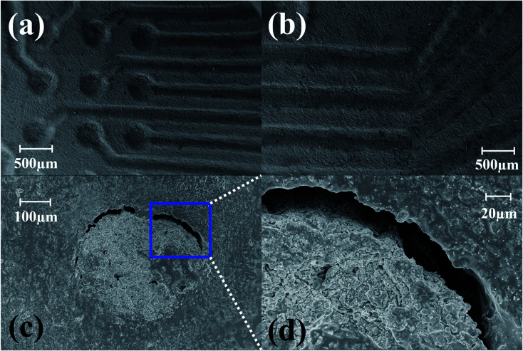
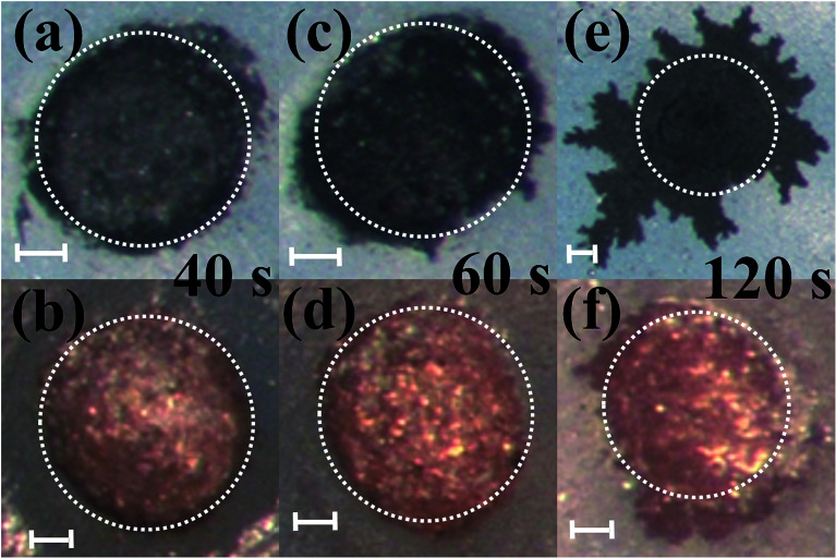
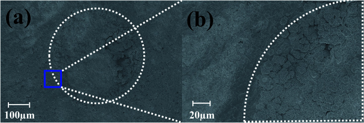
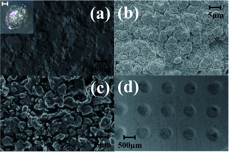
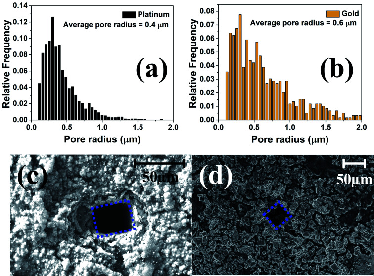
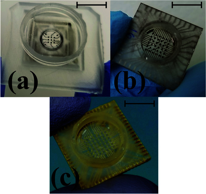
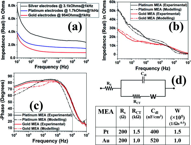
Conventional two-dimensional microelectrode arrays (2D MEAs) in the market involve long manufacturing timeframes, have cleanroom requirements, and need to be assembled from multiple parts to obtain the final packaged device. For MEAs to be "used and tossed", manufacturing has to be moved from the cleanroom to makerspaces. In order to enable makerspace fabricated MEAs comparable to conventional MEAs, the microfabrication processes must be optimized to have similar electrical properties along with biocompatibility and number of recording sites. This work presents a makerspace microfabricated 2D MEA having electrode densities up to a commercially popular 8 × 8 array, all fabricated under four days. Additive manufacturing-based realization of the MEA devices provides immense flexibility in terms of meeting distinct design requirements. A unique non-planar MEA having meso-scale electrodes on the top side of a chip transitioning to traces onto the bottom side through electrical vias is presented in this work. This allows for (a) monolithic integration of a culture well for devices having up to a 6 × 6 MEA array, (b) selective electroplating of the meso-scale electrodes (500 μm diameter) defined by silver ink casting followed by pulsed electroplating of gold or platinum without any masking procedure, (c) casting of a uniform and planar insulation layer a novel process of confined precision spin coating (CPSC) of SU-8 which acts as a biocompatible insulation atop the meso-scale electrodes; and (d) selective laser micromachining to define the 50 μm × 50 μm microelectrodes. For an 8 × 8 array, the culture well and MEA chip framework are 3D printed as two separate parts and sealed together with a biocompatible epoxy as in commercially available MEAs. The fabricated MEAs have an average 1 kHz impedance of 36.8 kΩ/16 kΩ with a double layer capacitance of 400 nF cm/520 nF cm for nano-porous platinum/nano-gold which is comparable to the state-of-art commercially available 2D MEAs. Additionally, it was found out that our 3D printing-based process compares very favorably with traditional glass MEAs in terms of design to device while representing a dramatic reduction in cost, timeline for fabrication, reduction in the number of steps and the need for sophisticated microfabrication and packaging equipment.

摘要

市面上传统的二维微电极阵列(2D MEA)制造时间长,有洁净室要求,且需由多个部件组装才能得到最终的封装器件。对于一次性使用的MEA,制造必须从洁净室转移到创客空间。为了使在创客空间制造的MEA能与传统MEA相媲美,必须优化微制造工艺,使其具有相似的电学性能以及生物相容性和记录位点数量。本文介绍了一种在创客空间微制造的2D MEA,其电极密度高达商业上常用的8×8阵列,且全部在四天内制造完成。基于增材制造实现MEA器件在满足不同设计要求方面提供了极大的灵活性。本文展示了一种独特的非平面MEA,芯片顶部有中尺度电极,通过电通孔过渡到底部的线路。这使得(a)对于具有高达6×6 MEA阵列的器件,能实现培养池的单片集成;(b)通过银墨铸造定义中尺度电极(直径500μm)后,对金或铂进行脉冲电镀选择性电镀中尺度电极,无需任何掩膜工艺;(c)铸造均匀且平面的绝缘层——一种新型的SU - 8受限精密旋涂(CPSC)工艺,该绝缘层在中尺度电极顶部起到生物相容性绝缘作用;以及(d)通过选择性激光微加工来定义50μm×50μm的微电极。对于8×8阵列,培养池和MEA芯片框架作为两个单独的部件进行3D打印,并像市售MEA一样用生物相容性环氧树脂密封在一起。制造的MEA对于纳米多孔铂/纳米金,平均1 kHz阻抗为36.8 kΩ/16 kΩ,双层电容为400 nF/cm/520 nF/cm,与市面上最先进的2D MEA相当。此外,研究发现,我们基于3D打印的工艺在从设计到器件方面与传统玻璃MEA相比具有很大优势,同时成本大幅降低、制造时间缩短、步骤数量减少,且无需复杂的微制造和封装设备。

https://cdn.ncbi.nlm.nih.gov/pmc/blobs/1445/9062012/650194b27127/c8ra09116a-f12.jpg
https://cdn.ncbi.nlm.nih.gov/pmc/blobs/1445/9062012/1be7112d6c78/c8ra09116a-f1.jpg
https://cdn.ncbi.nlm.nih.gov/pmc/blobs/1445/9062012/c7a859e7a885/c8ra09116a-f2.jpg
https://cdn.ncbi.nlm.nih.gov/pmc/blobs/1445/9062012/8cd870026efc/c8ra09116a-f3.jpg
https://cdn.ncbi.nlm.nih.gov/pmc/blobs/1445/9062012/a2b2de8df123/c8ra09116a-f4.jpg
https://cdn.ncbi.nlm.nih.gov/pmc/blobs/1445/9062012/75ec4a64b877/c8ra09116a-f5.jpg
https://cdn.ncbi.nlm.nih.gov/pmc/blobs/1445/9062012/2ae61a5b2982/c8ra09116a-f6.jpg
https://cdn.ncbi.nlm.nih.gov/pmc/blobs/1445/9062012/4c0d1336b378/c8ra09116a-f7.jpg
https://cdn.ncbi.nlm.nih.gov/pmc/blobs/1445/9062012/1748168bb759/c8ra09116a-f8.jpg
https://cdn.ncbi.nlm.nih.gov/pmc/blobs/1445/9062012/f94099dafb00/c8ra09116a-f9.jpg
https://cdn.ncbi.nlm.nih.gov/pmc/blobs/1445/9062012/0a2eb3eea433/c8ra09116a-f10.jpg
https://cdn.ncbi.nlm.nih.gov/pmc/blobs/1445/9062012/2ed1b7068585/c8ra09116a-f11.jpg
https://cdn.ncbi.nlm.nih.gov/pmc/blobs/1445/9062012/650194b27127/c8ra09116a-f12.jpg

相似文献

1
Optimization of makerspace microfabrication techniques and materials for the realization of planar, 3D printed microelectrode arrays in under four days.在四天内实现平面3D打印微电极阵列的创客空间微制造技术和材料的优化。
RSC Adv. 2019 Mar 18;9(16):8949-8963. doi: 10.1039/c8ra09116a. eCollection 2019 Mar 15.
2
Fabrication and Characterization of 3D Printed, 3D Microelectrode Arrays for Interfacing with a Peripheral Nerve-on-a-Chip.用于与片上周围神经接口的3D打印3D微电极阵列的制造与表征
ACS Biomater Sci Eng. 2021 Jul 12;7(7):3018-3029. doi: 10.1021/acsbiomaterials.0c01184. Epub 2020 Dec 10.
3
Makerspace microfabrication of a stainless steel 3D microneedle electrode array (3D MEA) on a glass substrate for simultaneous optical and electrical probing of electrogenic cells.在玻璃基板上通过创客空间微制造技术制备不锈钢3D微针电极阵列(3D MEA),用于对电生细胞进行同步光学和电学探测。
RSC Adv. 2020 Nov 18;10(68):41577-41587. doi: 10.1039/d0ra06070d. eCollection 2020 Nov 11.
4
Rapid Makerspace Microfabrication and Characterization of 3D Microelectrode Arrays (3D MEAs) for Organ-on-a-Chip Models.用于芯片器官模型的3D微电极阵列(3D MEA)的快速创客空间微制造与表征
J Microelectromech Syst. 2021;30(6):853-863. doi: 10.1109/jmems.2021.3110163. Epub 2021 Sep 15.
5
3D Printing, Ink Casting and Micromachined Lamination (3D PICLμM): A Makerspace Approach to the Fabrication of Biological Microdevices.3D打印、油墨铸造和微机械层压(3D PICLμM):一种用于制造生物微器件的创客空间方法。
Micromachines (Basel). 2018 Feb 15;9(2):85. doi: 10.3390/mi9020085.
6
Fabrication of Planar Microelectrode Array Using Laser-Patterned ITO and SU-8.使用激光图案化氧化铟锡(ITO)和SU-8制备平面微电极阵列
Micromachines (Basel). 2021 Oct 31;12(11):1347. doi: 10.3390/mi12111347.
7
Fully Printed μ-Needle Electrode Array from Conductive Polymer Ink for Bioelectronic Applications.全印刷导电聚合物墨水 μ 型针状电极阵列用于生物电子应用。
ACS Appl Mater Interfaces. 2019 Sep 11;11(36):32778-32786. doi: 10.1021/acsami.9b11774. Epub 2019 Aug 29.
8
Direct Growth of Carbon Nanotubes on New High-Density 3D Pyramid-Shaped Microelectrode Arrays for Brain-Machine Interfaces.用于脑机接口的新型高密度三维金字塔形微电极阵列上碳纳米管的直接生长
Micromachines (Basel). 2016 Sep 8;7(9):163. doi: 10.3390/mi7090163.
9
Carbon Nanotube-Based Printed All-Organic Microelectrode Arrays for Neural Stimulation and Recording.用于神经刺激和记录的基于碳纳米管的印刷全有机微电极阵列
Micromachines (Basel). 2024 May 14;15(5):650. doi: 10.3390/mi15050650.
10
Planar amorphous silicon carbide microelectrode arrays for chronic recording in rat motor cortex.用于大鼠运动皮层慢性记录的平面非晶硅碳化硅微电极阵列。
Biomaterials. 2024 Jul;308:122543. doi: 10.1016/j.biomaterials.2024.122543. Epub 2024 Mar 21.

引用本文的文献

1
Vat photopolymerization-based 3D printing of polymer nanocomposites: current trends and applications.基于光聚合反应的聚合物纳米复合材料3D打印:当前趋势与应用
RSC Adv. 2023 Jan 6;13(2):1456-1496. doi: 10.1039/d2ra06522c. eCollection 2023 Jan 3.
2
Makerspace microfabrication of a stainless steel 3D microneedle electrode array (3D MEA) on a glass substrate for simultaneous optical and electrical probing of electrogenic cells.在玻璃基板上通过创客空间微制造技术制备不锈钢3D微针电极阵列(3D MEA),用于对电生细胞进行同步光学和电学探测。
RSC Adv. 2020 Nov 18;10(68):41577-41587. doi: 10.1039/d0ra06070d. eCollection 2020 Nov 11.
3

本文引用的文献

1
3D-Printed Biosensor Arrays for Medical Diagnostics.用于医学诊断的3D打印生物传感器阵列
Micromachines (Basel). 2018 Aug 7;9(8):394. doi: 10.3390/mi9080394.
2
Extrusion-Based 3D Printing of Microfluidic Devices for Chemical and Biomedical Applications: A Topical Review.用于化学和生物医学应用的微流控装置的挤出式3D打印:综述
Micromachines (Basel). 2018 Jul 27;9(8):374. doi: 10.3390/mi9080374.
3
Micromachining on and of Transparent Polymers for Patterning Electrodes and Growing Electrically Active Cells for Biosensor Applications.
Realizing new designs of multiplexed electrode chips by 3-D printed masks.
通过3D打印掩膜实现复用电极芯片的新设计。
RSC Adv. 2021 Jun 17;11(35):21600-21606. doi: 10.1039/d1ra03482k. eCollection 2021 Jun 15.
4
Rapid Makerspace Microfabrication and Characterization of 3D Microelectrode Arrays (3D MEAs) for Organ-on-a-Chip Models.用于芯片器官模型的3D微电极阵列(3D MEA)的快速创客空间微制造与表征
J Microelectromech Syst. 2021;30(6):853-863. doi: 10.1109/jmems.2021.3110163. Epub 2021 Sep 15.
5
Capabilities and limitations of 3D printed microserpentines and integrated 3D electrodes for stretchable and conformable biosensor applications.用于可拉伸和贴合式生物传感器应用的3D打印微蛇形结构及集成3D电极的能力与局限性
Microsyst Nanoeng. 2020 Apr 20;6:15. doi: 10.1038/s41378-019-0129-3. eCollection 2020.
6
Inkjet-Printed and Electroplated 3D Electrodes for Recording Extracellular Signals in Cell Culture.喷墨打印和电镀 3D 电极用于细胞培养中的细胞外信号记录。
Sensors (Basel). 2021 Jun 9;21(12):3981. doi: 10.3390/s21123981.
7
Single-cell microfluidic impedance cytometry: from raw signals to cell phenotypes using data analytics.单细胞微流控阻抗细胞术:使用数据分析从原始信号到细胞表型。
Lab Chip. 2021 Jan 5;21(1):22-54. doi: 10.1039/d0lc00840k.
8
Micro/Nano Electrode Array Sensors: Advances in Fabrication and Emerging Applications in Bioanalysis.微/纳电极阵列传感器:制造技术进展及生物分析中的新兴应用
Front Chem. 2020 Nov 13;8:573865. doi: 10.3389/fchem.2020.573865. eCollection 2020.
9
Biocompatibility of Blank, Post-Processed and Coated 3D Printed Resin Structures with Electrogenic Cells.3D 打印树脂结构的空白、后处理和涂层的生物相容性与发电细胞。
Biosensors (Basel). 2020 Oct 22;10(11):152. doi: 10.3390/bios10110152.
10
Recent advances in three-dimensional microelectrode array technologies for in vitro and in vivo cardiac and neuronal interfaces.三维微电极阵列技术在体外和体内心脏及神经元接口中的最新进展。
Biosens Bioelectron. 2021 Jan 1;171:112687. doi: 10.1016/j.bios.2020.112687. Epub 2020 Oct 9.
用于生物传感器应用的透明聚合物上的微加工以及用于图案化电极和培养电活性细胞的微加工。
Micromachines (Basel). 2017 Aug 15;8(8):250. doi: 10.3390/mi8080250.
4
3D Printing, Ink Casting and Micromachined Lamination (3D PICLμM): A Makerspace Approach to the Fabrication of Biological Microdevices.3D打印、油墨铸造和微机械层压(3D PICLμM):一种用于制造生物微器件的创客空间方法。
Micromachines (Basel). 2018 Feb 15;9(2):85. doi: 10.3390/mi9020085.
5
ALS/FTD-Linked Mutation in FUS Suppresses Intra-axonal Protein Synthesis and Drives Disease Without Nuclear Loss-of-Function of FUS.ALS/FTD 相关突变 FUS 抑制轴内蛋白合成并驱动疾病,而不导致 FUS 的核功能丧失。
Neuron. 2018 Nov 21;100(4):816-830.e7. doi: 10.1016/j.neuron.2018.09.044. Epub 2018 Oct 18.
6
Rapid Nanofabrication of Nanostructured Interdigitated Electrodes (nIDEs) for Long-Term In Vitro Analysis of Human Induced Pluripotent Stem Cell Differentiated Cardiomyocytes.快速纳米制造纳米结构叉指电极(nIDEs)用于人类诱导多能干细胞分化的心肌细胞的长期体外分析。
Biosensors (Basel). 2018 Oct 11;8(4):88. doi: 10.3390/bios8040088.
7
Convergent Pathways in Idiopathic Autism Revealed by Time Course Transcriptomic Analysis of Patient-Derived Neurons.特发性自闭症患者来源神经元时间进程转录组分析揭示的汇聚途径。
Sci Rep. 2018 May 30;8(1):8423. doi: 10.1038/s41598-018-26495-1.
8
Na1.7 as a Pharmacogenomic Target for Pain: Moving Toward Precision Medicine.钠离子通道 1.7 作为疼痛的药物基因组靶点:迈向精准医学。
Trends Pharmacol Sci. 2018 Mar;39(3):258-275. doi: 10.1016/j.tips.2017.11.010. Epub 2018 Jan 20.
9
In vitro biocompatibility and electrical stability of thick-film platinum/gold alloy electrodes printed on alumina.印刷在氧化铝上的厚膜铂/金合金电极的体外生物相容性和电稳定性
J Neural Eng. 2017 Jun;14(3):036012. doi: 10.1088/1741-2552/aa6557. Epub 2017 Mar 8.
10
Ceramic-Based Multisite Platinum Microelectrode Arrays: Morphological Characteristics and Electrochemical Performance for Extracellular Oxygen Measurements in Brain Tissue.基于陶瓷的多部位铂微电极阵列:用于脑组织细胞外氧测量的形态特征和电化学性能。
Anal Chem. 2017 Feb 7;89(3):1674-1683. doi: 10.1021/acs.analchem.6b03772. Epub 2017 Jan 25.