Department of Materials Science and Engineering, City University of Hong Kong, Kowloon, 999077, Hong Kong SAR.
State Key Laboratory of Terahertz and Millimeter Waves, City University of Hong Kong, Kowloon, 999077, Hong Kong SAR.
Nat Commun. 2023 Apr 27;14(1):2431. doi: 10.1038/s41467-023-38090-8.
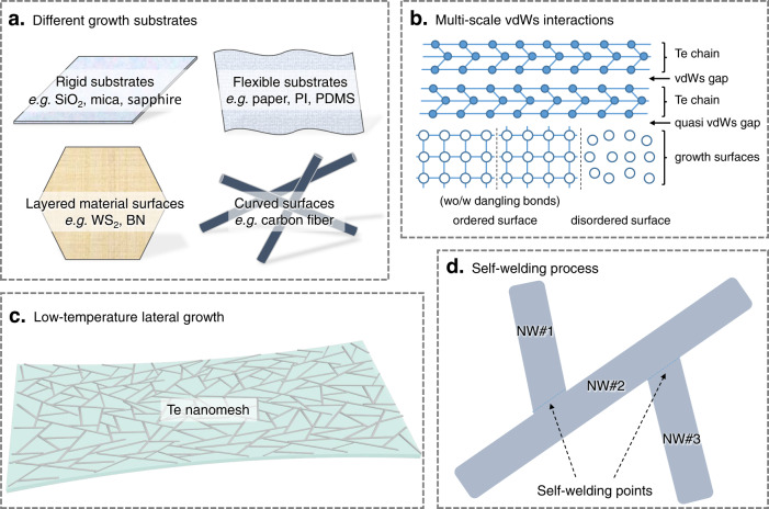
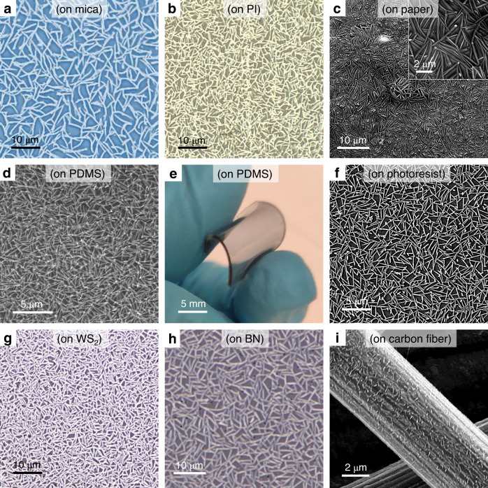
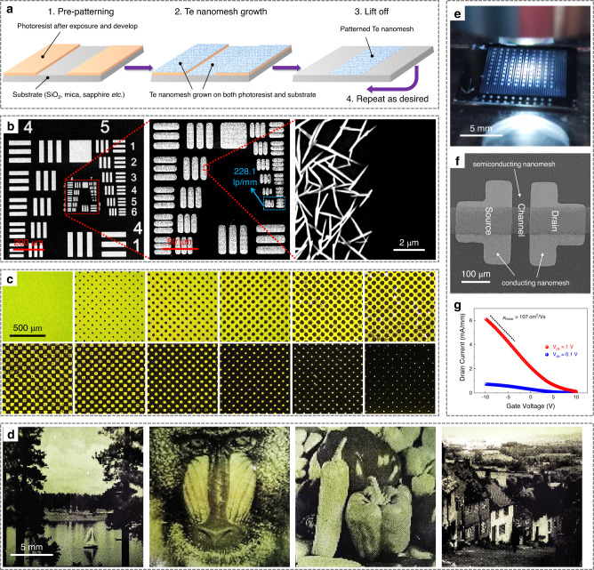
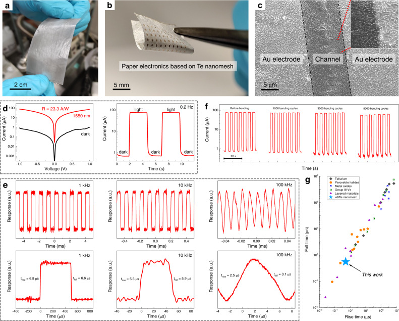
Chemical bonds, including covalent and ionic bonds, endow semiconductors with stable electronic configurations but also impose constraints on their synthesis and lattice-mismatched heteroepitaxy. Here, the unique multi-scale van der Waals (vdWs) interactions are explored in one-dimensional tellurium (Te) systems to overcome these restrictions, enabled by the vdWs bonds between Te atomic chains and the spontaneous misfit relaxation at quasi-vdWs interfaces. Wafer-scale Te vdWs nanomeshes composed of self-welding Te nanowires are laterally vapor grown on arbitrary surfaces at a low temperature of 100 °C, bringing greater integration freedoms for enhanced device functionality and broad applicability. The prepared Te vdWs nanomeshes can be patterned at the microscale and exhibit high field-effect hole mobility of 145 cm/Vs, ultrafast photoresponse below 3 μs in paper-based infrared photodetectors, as well as controllable electronic structure in mixed-dimensional heterojunctions. All these device metrics of Te vdWs nanomesh electronics are promising to meet emerging technological demands.
化学键,包括共价键和离子键,赋予半导体稳定的电子构型,但也对它们的合成和晶格失配异质外延施加了限制。在这里,探索了一维碲(Te)系统中独特的多尺度范德华(vdWs)相互作用,以克服这些限制,这得益于 Te 原子链之间的 vdWs 键和准 vdWs 界面处的自发失配弛豫。由自焊接 Te 纳米线组成的晶圆级 Te vdWs 纳米网在 100°C 的低温下在任意表面上横向汽相生长,为增强器件功能和广泛适用性带来了更大的集成自由度。制备的 Te vdWs 纳米网可以在微尺度上进行图案化,并表现出高达 145cm/Vs 的高场效应空穴迁移率、在基于纸张的红外光电探测器中低于 3μs 的超快光响应,以及在混合维度异质结中可控制的电子结构。Te vdWs 纳米网电子的所有这些器件指标都有望满足新兴技术需求。